As component densities on printed circuit board assemblies continue to rise and solder joint geometries shrink, visual inspection by human operators has long ceased to be a viable sole quality assurance method. Automated Optical Inspection — universally abbreviated as AOI — addresses this challenge by combining high-resolution camera systems, structured illumination and image-processing algorithms to detect assembly defects at throughput rates no human inspector can match. Despite being a well-established technology, AOI is frequently misunderstood in its scope: it is neither a universal defect detector nor a simple pass/fail camera. Its correct application depends on a solid grasp of its operating principles, its genuine capabilities and its inherent limitations.
Within a modern SMT line, AOI systems are typically deployed at two or more process stages: after solder paste printing (though dedicated SPI systems are more common here), after component placement and, most critically, after reflow soldering. Each inspection point catches a different defect spectrum and allows corrective action before additional value is added to the assembly. This staged approach is central to the economic argument for AOI: the later a defect is discovered, the more costly its correction becomes.
Illumination and Image Acquisition: The Optical Foundation
The optical subsystem is the heart of any AOI machine. Most contemporary systems use area-scan or line-scan cameras in combination with multi-directional, multi-wavelength LED illumination. Angled illumination from several directions — often arranged in concentric rings at different elevation angles — creates characteristic highlight and shadow patterns on solder menisci, component bodies and PCB pads. These patterns are far more information-rich than images taken under flat, diffuse light. Colour information from red, green and blue illumination channels helps discriminate between copper, solder, solder mask and component surface materials, all of which have distinct reflectance characteristics.
3D AOI, now widely adopted in higher-end systems, extends this principle by adding structured-light projection — typically fringe projection or laser triangulation — to generate height maps of the PCB surface. This third dimension is particularly valuable for solder joint inspection: a joint may appear geometrically correct in a 2D top-down image yet still exhibit insufficient solder volume or coplanarity issues that only become apparent in the height data. The combination of 2D colour imaging and 3D topography significantly reduces both false-call rates and escape rates compared to 2D-only systems.
Defect Detection: What AOI Can and Cannot Find
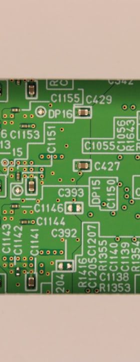
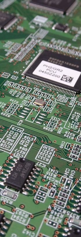
AOI excels at detecting surface-visible defects. Missing components, wrong component types or values (where markings are legible on the top surface), misalignment, tombstoning, solder bridges between adjacent pads, insufficient solder, lifted leads on flat-pack devices and certain types of solder balling are all within the reliable detection envelope of a well-programmed system. After reflow, solder joint shape analysis — wetting angle, fillet height, pad coverage — is performed by comparing the acquired image or point cloud against reference models derived from the inspection programme.
However, AOI cannot inspect what it cannot see. Solder joints hidden beneath component bodies — such as the balls of a BGA, the terminations of a QFN or the contacts of a bottom-terminated component — are optically inaccessible. Internal voids within solder joints, cold joints with acceptable external geometry and opens beneath area-array packages fall outside AOI's detection capability. For these defects, Automated X-ray Inspection (AXI) or a combination of AXI and electrical test methods is required. Recognising this boundary is crucial when designing a test strategy: AOI and AXI are complementary rather than interchangeable technologies.
Programming, Thresholds and the False-Call Problem
The practical effectiveness of an AOI system is determined less by its hardware than by the quality of its inspection programme and the calibration of its acceptance thresholds. Inspection programmes are typically generated from Gerber data, component placement files and a library of component models, then refined through a teach-in or golden-board process. Each inspection feature — pad coverage, component presence, polarity marker orientation — is associated with a tolerance window. Setting these windows too tightly produces excessive false calls (pseudo-errors), which overwhelm repair operators, erode confidence in the system and ultimately lead to alarm fatigue. Setting them too loosely allows genuine defects to escape.
Modern AOI platforms address this trade-off through statistical process feedback: escape and false-call events recorded at downstream inspection and repair stations are fed back into the AOI programme to iteratively tighten or relax individual thresholds. Some systems incorporate machine-learning classifiers trained on large annotated defect image datasets, which can generalise across board variants and reduce the manual optimisation burden. Regardless of algorithmic sophistication, a structured programme verification process — including deliberate introduction of known defects during initial setup — remains best practice.
Integration into the SMT Line and Closed-Loop Process Control
AOI is most powerful when it is not operated as a standalone quality gate but is tightly coupled to upstream and downstream process equipment via a manufacturing execution system (MES) or process control software. Statistical data gathered by the AOI — defect counts per board, defect location heat maps, trend analysis across production lots — can be used to identify systematic process drift long before it breaches outright rejection limits. A recurring pattern of solder bridges on a specific pad pair, for instance, may indicate a stencil aperture that requires cleaning or redesign, a printer alignment drift or a reflow profile anomaly.
Closed-loop feedback to the solder paste printer — automatically adjusting print parameters in response to AOI data — is an established practice in high-volume lines. Similar feedback paths to reflow oven profile management and component placement machines are increasingly supported by equipment suppliers. This shift from reactive defect detection to proactive process control represents the most significant evolution in AOI's role within the smart factory concept, transforming the inspection system from a quality filter into an active process monitoring node.
Selecting the Right System: Key Criteria for the Purchasing Decision
When evaluating AOI systems, several technical parameters require careful comparison. Optical resolution — expressed as the minimum detectable feature size, typically in micrometres per pixel — must be matched to the smallest component and pitch on the board. For assemblies with 0201 metric components or fine-pitch ICs at 0.4 mm pitch, resolutions below 10 µm per pixel are generally necessary. Field of view determines throughput: a larger field of view reduces the number of camera positions required to cover a full board but may compromise resolution. The balance between these two parameters is a fundamental design trade-off in any AOI platform.
Cycle time compatibility with line takt, conveyor width range, software openness for MES integration and the vendor's library coverage for current and emerging component packages are equally important evaluation criteria. In high-mix, low-volume environments, rapid programme changeover capability and the effort required to create new inspection programmes per board variant become decisive factors. Prospective users should request benchmark tests on representative boards from their own product portfolio rather than relying solely on manufacturer-specified capability claims.
Practical Outlook: Towards AI-Assisted Inspection
The trajectory of AOI development points clearly towards greater use of deep-learning-based defect classification, moving beyond rule-based comparison to models capable of detecting novel defect morphologies and adapting to new component types with reduced training effort. Alongside this, the integration of AOI data into broader digital twin and Industry 4.0 frameworks will deepen: inspection results linked to individual board serial numbers, specific paste lot data, placement machine head assignments and reflow oven zone temperatures create a traceable dataset that supports both root-cause analysis and predictive quality management. For electronics manufacturers, the priority is not simply to procure an AOI system but to embed it as an intelligent node within a data-driven production environment — a prerequisite for sustaining quality in increasingly complex assemblies.