
Zum Inhalt springen
EPP Europe
  • News
  • Products
  • Applications
  • Technology
  • Semiconductor
  • Inspection
  • Company News
  • Events
EPP Europe
  • Technology
  • Inspection (AOI/AXI)
  • Semiconductor Packaging
  • Company News
  • Products
  • Trade Shows & Events
    EPP Europe Newsletter
    The most important electronics-manufacturing news delivered to your inbox.

    Info

    • Impressum
    • Datenschutz
    • Barrierefreiheit
    • Datenschutzeinstellungen

    Kontakt zur Redaktion

    EPP EuropeKonradin Mediengruppe
    Ernst-Mey-Str. 8, 70771 Leinfelden-Echterdingen

    E-Mail: redaktion@konradin.de
    Folgen Sie uns
    EPP Europe
    © 2026 EPP Europe
    Startseite/Semiconductor-packaging/Artikel
    ASMPT opens European semiconductor compentence centre
    Bildquelle nicht angegeben
    Semiconductor-packaging

    ASMPT opens European semiconductor compentence centre

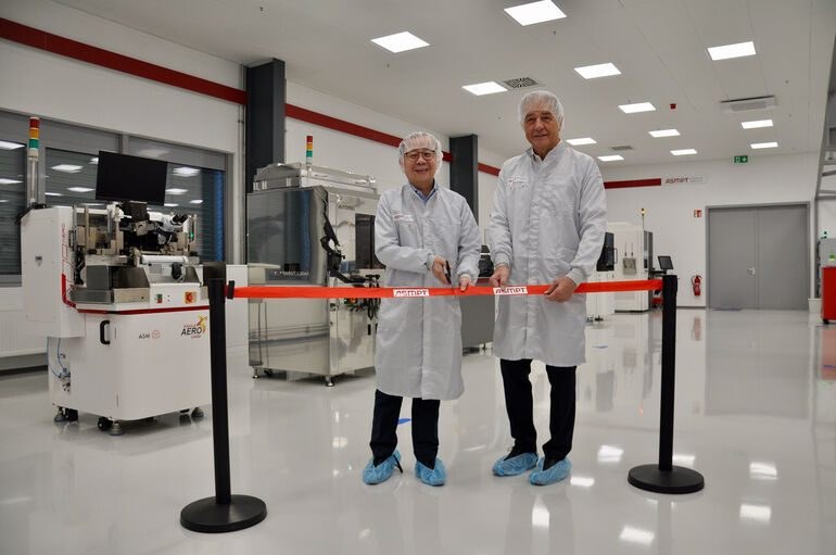
    ASMPT, a leading provider of hardware and software solutions for semiconductor and electronics manufacturing, has opened its first European semiconductor
    Veröffentlicht
    27. Januar 2023
    Lesezeit
    2 Minuten
    Rubrik
    Semiconductor-packaging

    Robin Ng, the Group‘s Chief Executive Officer, opened the new Center at the headquarters of ASMPT‘s subsidiary AMICRA in Regensburg, Germany. “Our customers expect a local presence for their research and development and fast, competent know-how transfer,” he said. “With our new EU SEMI CoC, we support our numerous customers in the development and design of new applications and ensure that new technologies also prove themselves in practice. We see a lot of potential in Germany, especially in the automotive and photonics sectors.”

    “We are pleased that we can now offer leading semiconductor companies and decision-makers in Europe the innovative ASMPT Semiconductor solutions and know-how in our centrally located CoC in Germany,“ said Dr. Johann Weinhändler, Managing Director of AMICRA.

    Resilient to supply chain disruptions

    The company says the new Center follows a successful corporate philosophy of strict customer orientation and offers protection against the overall increase in volatility in the global electronics supply chain. “ASMPT sees its role not only as a leading supplier to the semiconductor and electronics industry worldwide, but also as an innovation driver for manufacturing processes,” explained Günter Lauber, Executive Vice President, Chief Strategy and Digitalization Officer and SMT Segment CEO, ASMPT. “For this reason alone, it is important for us to further expand our already significant investments in research and development worldwide.“

    Proof of Concepts for Industry 4.0

    ASMPT operates a large network of research and development centers globally. These are modern and forward-looking laboratories with the latest machinery and equipment to demonstrate technologies and investigate the precise impact that innovations will have in electronics manufacturing. Customers can tell the experts at the CoC what interests them and what aspects are relevant to their individual production. Through close technology partnerships with other companies, the company says its Centers of Competence also act as enablers for the Integrated Smart Factory.


    www.asm-smt.com

    Mehr aus Semiconductor-packaging

    Weitere aktuelle Artikel aus der Rubrik Semiconductor-packaging.

    Alle Semiconductor-packaging-Artikel
    Nanoscribe Expands Photoresin Portfolio for Micro-Optics Fabrication via Two-Photon PolymerizationFoto: Brecht Corbeel / Unsplash
    Semiconductor-packaging

    Nanoscribe Expands Photoresin Portfolio for Micro-Optics Fabrication via Two-Photon Polymerization

    11. November 2026

    Nanoscribe has detailed its range of photoresins engineered for Two-Photon Polymerization (2PP) and Two-Photon Grayscale Lithography (2GL), targeting high-precision micro-optics manufacturing on silicon, glass, and…

    Canon Launches FPA-6400ES6a KrF Lithography System with 400 Wafers-per-Hour ThroughputFoto: Canon Europe (semicon)
    Semiconductor-packaging

    Canon Launches FPA-6400ES6a KrF Lithography System with 400 Wafers-per-Hour Throughput

    10. November 2026

    Canon has announced the FPA-6400ES6a KrF scanner for semiconductor lithography, combining a throughput of 400 wafers per hour with industry-leading overlay accuracy of 4.0 nm and the ability to handle wafer warpage of…

    Fabmatics absorbs SCI business activities under unified brandFoto: Ludovico Ceroseis / Unsplash
    Semiconductor-packaging

    Fabmatics absorbs SCI business activities under unified brand

    6. November 2026

    Fabmatics has integrated the business activities of SCI under the Fabmatics brand, consolidating the acquired expertise within its semiconductor automation portfolio.

    Entegris and Kioxia Expand Partnership on Materials Innovation for Next-Gen 3D Flash MemoryFoto: Louis Reed / Unsplash
    Semiconductor-packaging

    Entegris and Kioxia Expand Partnership on Materials Innovation for Next-Gen 3D Flash Memory

    6. November 2026

    Entegris and Kioxia are deepening their strategic partnership to co-develop materials and process technologies for future BiCS FLASH 3D NAND architectures, using AI, digital-twin modelling and experimental validation at…

    ← Zurück zu Semiconductor-packagingZur Startseite

