
Zum Inhalt springen
EPP Europe
  • News
  • Products
  • Applications
  • Technology
  • Semiconductor
  • Inspection
  • Company News
  • Events
EPP Europe
  • Technology
  • Inspection (AOI/AXI)
  • Semiconductor Packaging
  • Company News
  • Products
  • Trade Shows & Events
    EPP Europe Newsletter
    The most important electronics-manufacturing news delivered to your inbox.

    Info

    • Impressum
    • Datenschutz
    • Barrierefreiheit
    • Datenschutzeinstellungen

    Kontakt zur Redaktion

    EPP EuropeKonradin Mediengruppe
    Ernst-Mey-Str. 8, 70771 Leinfelden-Echterdingen

    E-Mail: redaktion@konradin.de
    Folgen Sie uns
    EPP Europe
    © 2026 EPP Europe
    Startseite/Semiconductor-packaging/Artikel
    Applying 3D Moiré Interferometry Measurement to SemiCon Applications
    Bildquelle nicht angegeben
    Semiconductor-packaging

    Applying 3D Moiré Interferometry Measurement to SemiCon Applications

    Due to the shortage of components in the electronics industry and the dependence on Asian suppliers, the European Community has decided to double Europe's
    Veröffentlicht
    19. August 2022
    Lesezeit
    1 Minute
    Rubrik
    Semiconductor-packaging

    At the same time, we are seeing a trend toward multi-chip packaging. Moore’s Law no longer applies. The cost of developing smaller structures is too high, but the possibilities and advantages of combining different chips and components in one package are promising. Complex functions of entire devices can be integrated into a small BGA or IC package. This trend affects all packaging processes from 2D to 3D to wafer-level packaging.

    The packaging process is becoming more complex and challenging, but new interconnect methods such as hybrid bonding and interposer materials are enabling higher density and higher levels of integration. Smaller components, higher density and new materials are challenging existing inspection and measurement systems. Customized measurement equipment is needed to support the new packaging trends. Especially when the boundaries between front-end and back-end applications or back-end and SMT become blurred.

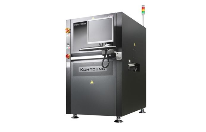
    3D Moiré interferometry measurement is the latest standard in SMT. Due to the proven robustness and reliability of this measurement, these machines have been used in semiconductor packaging for several years.The online seminar shows the adaptation of the well-known Moiré interferometry principle in SemiCon and packaging applications.

    More useful information to be received during a KohYoung webinar on September 15, 11:00 am. For an immediate registration please click here.


    Mehr aus Semiconductor-packaging

    Weitere aktuelle Artikel aus der Rubrik Semiconductor-packaging.

    Alle Semiconductor-packaging-Artikel
    Nanoscribe Expands Photoresin Portfolio for Micro-Optics Fabrication via Two-Photon PolymerizationFoto: Brecht Corbeel / Unsplash
    Semiconductor-packaging

    Nanoscribe Expands Photoresin Portfolio for Micro-Optics Fabrication via Two-Photon Polymerization

    11. November 2026

    Nanoscribe has detailed its range of photoresins engineered for Two-Photon Polymerization (2PP) and Two-Photon Grayscale Lithography (2GL), targeting high-precision micro-optics manufacturing on silicon, glass, and…

    Canon Launches FPA-6400ES6a KrF Lithography System with 400 Wafers-per-Hour ThroughputFoto: Canon Europe (semicon)
    Semiconductor-packaging

    Canon Launches FPA-6400ES6a KrF Lithography System with 400 Wafers-per-Hour Throughput

    10. November 2026

    Canon has announced the FPA-6400ES6a KrF scanner for semiconductor lithography, combining a throughput of 400 wafers per hour with industry-leading overlay accuracy of 4.0 nm and the ability to handle wafer warpage of…

    Fabmatics absorbs SCI business activities under unified brandFoto: Ludovico Ceroseis / Unsplash
    Semiconductor-packaging

    Fabmatics absorbs SCI business activities under unified brand

    6. November 2026

    Fabmatics has integrated the business activities of SCI under the Fabmatics brand, consolidating the acquired expertise within its semiconductor automation portfolio.

    Entegris and Kioxia Expand Partnership on Materials Innovation for Next-Gen 3D Flash MemoryFoto: Louis Reed / Unsplash
    Semiconductor-packaging

    Entegris and Kioxia Expand Partnership on Materials Innovation for Next-Gen 3D Flash Memory

    6. November 2026

    Entegris and Kioxia are deepening their strategic partnership to co-develop materials and process technologies for future BiCS FLASH 3D NAND architectures, using AI, digital-twin modelling and experimental validation at…

    ← Zurück zu Semiconductor-packagingZur Startseite

