
Zum Inhalt springen
EPP Europe
  • News
  • Products
  • Applications
  • Technology
  • Semiconductor
  • Inspection
  • Company News
  • Events
EPP Europe
  • Technology
  • Inspection (AOI/AXI)
  • Semiconductor Packaging
  • Company News
  • Products
  • Trade Shows & Events
    EPP Europe Newsletter
    The most important electronics-manufacturing news delivered to your inbox.

    Info

    • Impressum
    • Datenschutz
    • Barrierefreiheit
    • Datenschutzeinstellungen

    Kontakt zur Redaktion

    EPP EuropeKonradin Mediengruppe
    Ernst-Mey-Str. 8, 70771 Leinfelden-Echterdingen

    E-Mail: redaktion@konradin.de
    Folgen Sie uns
    EPP Europe
    © 2026 EPP Europe
    Startseite/Semiconductor-packaging/Artikel
    Ankineedu Velaga to Lead YES India as Country Head and Managing Director
    Bildquelle nicht angegeben
    Semiconductor-packaging

    Ankineedu Velaga to Lead YES India as Country Head and Managing Director

    YES (Yield Engineering Systems, Inc.), a leading manufacturer of process equipment for semiconductor advanced packaging, life sciences and
    Veröffentlicht
    08. April 2022
    Lesezeit
    2 Minuten
    Rubrik
    Semiconductor-packaging

    “It is no secret that high-caliber engineering expertise is in high demand in Silicon Valley,” said Ramakanth Alapati, Chairman and CEO of YES. “Our company’s rapid growth has inspired us to widen our technical recruitment efforts to include global engineering talent powerhouses like India. In addition, we feel there is a strong market for reliable, cost-effective YES systems within India’s domestic semiconductor industry.”

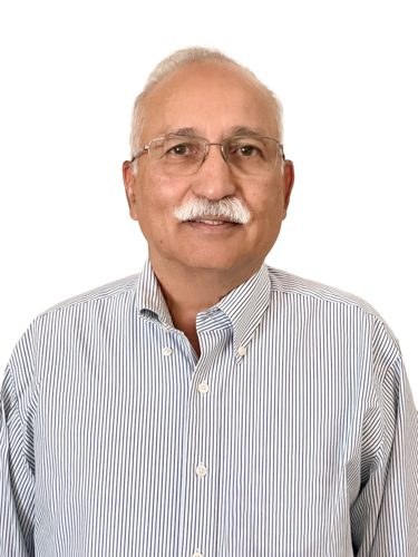
    Leading YES’s efforts in India will be Dr. Ankineedu Velaga, a high-tech engineering executive with more than 35 years of experience spanning engineering and fab operations, customer interaction and retention, and business development support in the US and Asia. “I am pleased and honored to be embarking on this exciting endeavor with YES,” commented Velaga.

    “Ankineedu’s experience in driving teams to improve processes will be a great resource for YES as we scale to meet the challenges of worldwide growth. We will be looking to him to draw upon his impressive track record of building organizations to develop complex semiconductor capital equipment as well as leading organizations to achieve better process development, yields, process control, cycle time, cost, and product quality,” said Rezwan Lateef, President of YES.

    Dr. Velaga has held leadership roles with BRIDG, imec, SilTerra, Applied Materials, Avago, and Lucent (among others), and his global management experience extends from the US and the European Union to Malaysia and Singapore. His educational background includes a Ph.D. in Chemical Engineering from the University of Arkansas, an M.S. in Chemical Engineering from the Indian Institute of Technology in Madras, and a B.S in Chemical Engineering from the Regional Engineering College in Warangal, India.


    Mehr aus Semiconductor-packaging

    Weitere aktuelle Artikel aus der Rubrik Semiconductor-packaging.

    Alle Semiconductor-packaging-Artikel
    Kosmek Publishes Semiconductor Manufacturing Automation CatalogFoto: Kosmek (semicon)
    Semiconductor-packaging

    Kosmek Publishes Semiconductor Manufacturing Automation Catalog

    13. November 2026

    Kosmek has released an industrial automation catalog focused on semiconductor manufacturing, detailing pneumatic supports, robotic hand changers and locating components applicable across front-end and back-end…

    Nanoscribe Expands Photoresin Portfolio for Micro-Optics Fabrication via Two-Photon PolymerizationFoto: Brecht Corbeel / Unsplash
    Semiconductor-packaging

    Nanoscribe Expands Photoresin Portfolio for Micro-Optics Fabrication via Two-Photon Polymerization

    11. November 2026

    Nanoscribe has detailed its range of photoresins engineered for Two-Photon Polymerization (2PP) and Two-Photon Grayscale Lithography (2GL), targeting high-precision micro-optics manufacturing on silicon, glass, and…

    Canon Launches FPA-6400ES6a KrF Lithography System with 400 Wafers-per-Hour ThroughputFoto: Canon Europe (semicon)
    Semiconductor-packaging

    Canon Launches FPA-6400ES6a KrF Lithography System with 400 Wafers-per-Hour Throughput

    10. November 2026

    Canon has announced the FPA-6400ES6a KrF scanner for semiconductor lithography, combining a throughput of 400 wafers per hour with industry-leading overlay accuracy of 4.0 nm and the ability to handle wafer warpage of…

    Fabmatics absorbs SCI business activities under unified brandFoto: Ludovico Ceroseis / Unsplash
    Semiconductor-packaging

    Fabmatics absorbs SCI business activities under unified brand

    6. November 2026

    Fabmatics has integrated the business activities of SCI under the Fabmatics brand, consolidating the acquired expertise within its semiconductor automation portfolio.

    ← Zurück zu Semiconductor-packagingZur Startseite

