
Zum Inhalt springen
EPP Europe
  • News
  • Products
  • Applications
  • Technology
  • Semiconductor
  • Inspection
  • Company News
  • Events
EPP Europe
  • Technology
  • Inspection (AOI/AXI)
  • Semiconductor Packaging
  • Company News
  • Products
  • Trade Shows & Events
    EPP Europe Newsletter
    The most important electronics-manufacturing news delivered to your inbox.

    Info

    • Impressum
    • Datenschutz
    • Barrierefreiheit
    • Datenschutzeinstellungen

    Kontakt zur Redaktion

    EPP EuropeKonradin Mediengruppe
    Ernst-Mey-Str. 8, 70771 Leinfelden-Echterdingen

    E-Mail: redaktion@konradin.de
    Folgen Sie uns
    EPP Europe
    © 2026 EPP Europe
    Startseite/Semiconductor-packaging/Artikel
    Addition to Ontos Family of Acoustic Metrology Products
    Bildquelle nicht angegeben
    Semiconductor-packaging

    Addition to Ontos Family of Acoustic Metrology Products

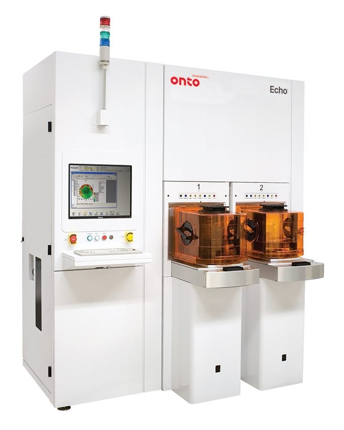
    Onto announced the next evolutionary step of innovative acoustic metrology products. The new Echo system further expands the addressable market for
    Veröffentlicht
    12. Juli 2022
    Lesezeit
    2 Minuten
    Rubrik
    Semiconductor-packaging

    Operating at three times the signal-to-noise ratio (SNR) of existing products, the Echo system supports a wide range of film thicknesses, from
    very thin 50Å films up to 35μm opaque films and metal layers. Furthermore, the Echo system has materials characterization capabilities that include in-line time domain thermo-reëectance for implant monitoring and thermal conductivity characterization.

    “By leveraging Onto’s tool-centric software, the Echo system oéers a complete solution at HVM customer sites where on-wafer metrology measurements are used in a closed loop feedback approach to enact run-to-run process control on key enabling film deposition steps,” said Danielle Baptiste, vice president and general manager of Onto Innovation’s enterprise software business.

    “As tier stacks in vertical NAND devices continue to grow, key deposition steps, such as the hard mask, are critical to the channel hole formation process. The accurate thickness and mechanical properties of these films are extremely critical to ensure that the film maintains integrity throughout the etch process,” said Priya Mukundhan, senior director of product management at Onto Innovation.

    Early adoption of the Echo system has been quite strong at a variety of customers and is entering these new
    markets with an order backlog of $20 million.

    Mehr aus Semiconductor-packaging

    Weitere aktuelle Artikel aus der Rubrik Semiconductor-packaging.

    Alle Semiconductor-packaging-Artikel
    Nanoscribe Expands Photoresin Portfolio for Micro-Optics Fabrication via Two-Photon PolymerizationFoto: Brecht Corbeel / Unsplash
    Semiconductor-packaging

    Nanoscribe Expands Photoresin Portfolio for Micro-Optics Fabrication via Two-Photon Polymerization

    11. November 2026

    Nanoscribe has detailed its range of photoresins engineered for Two-Photon Polymerization (2PP) and Two-Photon Grayscale Lithography (2GL), targeting high-precision micro-optics manufacturing on silicon, glass, and…

    Canon Launches FPA-6400ES6a KrF Lithography System with 400 Wafers-per-Hour ThroughputFoto: Canon Europe (semicon)
    Semiconductor-packaging

    Canon Launches FPA-6400ES6a KrF Lithography System with 400 Wafers-per-Hour Throughput

    10. November 2026

    Canon has announced the FPA-6400ES6a KrF scanner for semiconductor lithography, combining a throughput of 400 wafers per hour with industry-leading overlay accuracy of 4.0 nm and the ability to handle wafer warpage of…

    Fabmatics absorbs SCI business activities under unified brandFoto: Ludovico Ceroseis / Unsplash
    Semiconductor-packaging

    Fabmatics absorbs SCI business activities under unified brand

    6. November 2026

    Fabmatics has integrated the business activities of SCI under the Fabmatics brand, consolidating the acquired expertise within its semiconductor automation portfolio.

    Entegris and Kioxia Expand Partnership on Materials Innovation for Next-Gen 3D Flash MemoryFoto: Louis Reed / Unsplash
    Semiconductor-packaging

    Entegris and Kioxia Expand Partnership on Materials Innovation for Next-Gen 3D Flash Memory

    6. November 2026

    Entegris and Kioxia are deepening their strategic partnership to co-develop materials and process technologies for future BiCS FLASH 3D NAND architectures, using AI, digital-twin modelling and experimental validation at…

    ← Zurück zu Semiconductor-packagingZur Startseite


