
Zum Inhalt springen
EPP Europe
  • News
  • Products
  • Applications
  • Technology
  • Semiconductor
  • Inspection
  • Company News
  • Events
EPP Europe
  • Technology
  • Inspection (AOI/AXI)
  • Semiconductor Packaging
  • Company News
  • Products
  • Trade Shows & Events
    EPP Europe Newsletter
    The most important electronics-manufacturing news delivered to your inbox.

    Info

    • Impressum
    • Datenschutz
    • Barrierefreiheit
    • Datenschutzeinstellungen

    Kontakt zur Redaktion

    EPP EuropeKonradin Mediengruppe
    Ernst-Mey-Str. 8, 70771 Leinfelden-Echterdingen

    E-Mail: redaktion@konradin.de
    Folgen Sie uns
    EPP Europe
    © 2026 EPP Europe
    Startseite/Semiconductor-packaging/Artikel
    Acquisition expands product range
    Bildquelle nicht angegeben
    Semiconductor-packaging

    Acquisition expands product range

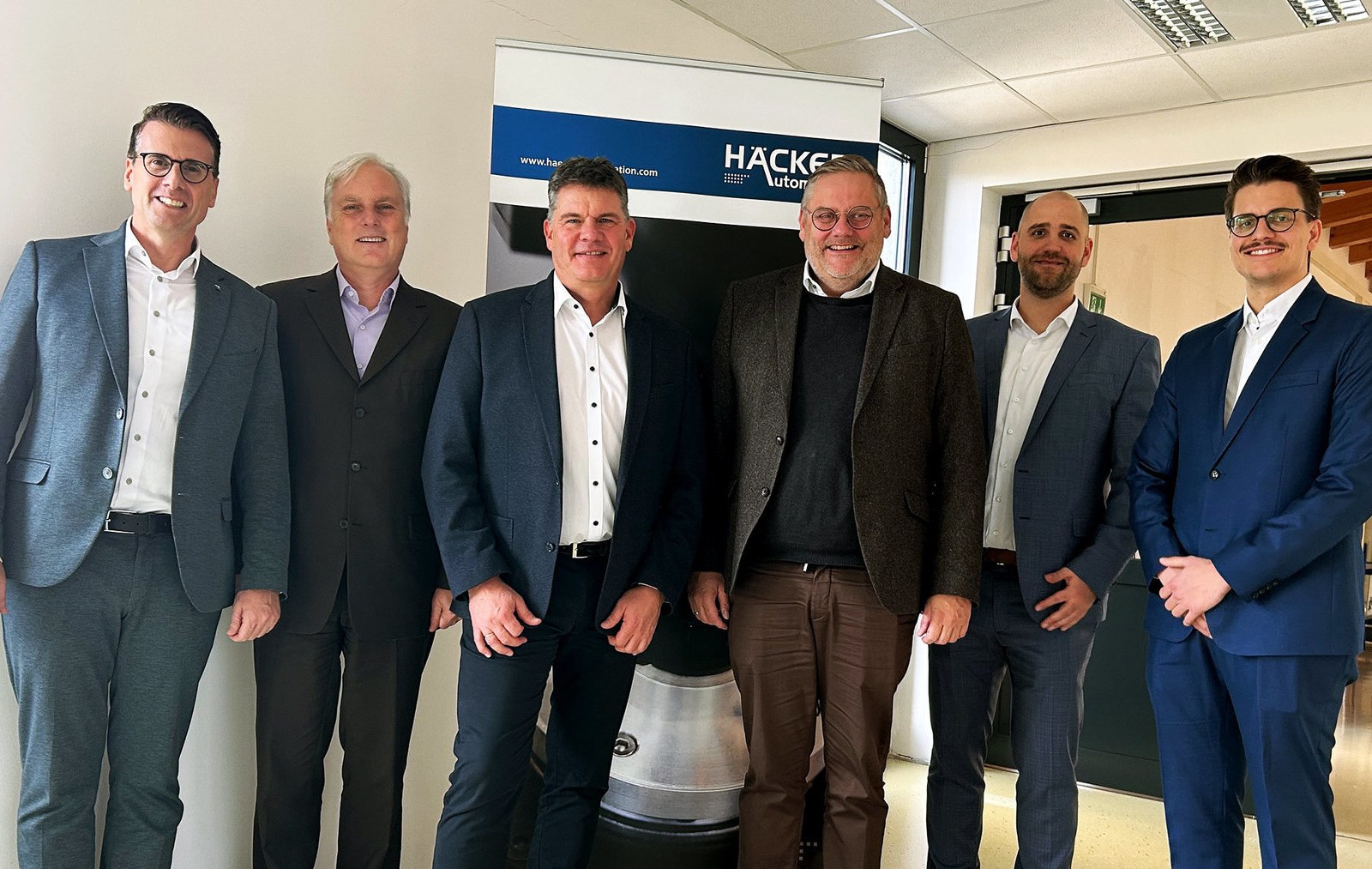
    Kurtz Ersa sharpened its focus on process technologies for microelectronics and microoptics with the takeover of Häcker Automation in December 2025. Häcker Automation is based in Waltershausen in the German state of Thuringia and has been producing microassembly systems for renowned customers in the semiconductor,…
    Veröffentlicht
    23. Januar 2026
    Lesezeit
    2 Minuten
    Rubrik
    Semiconductor-packaging

    Kurtz Ersa sharpened its focus on process technologies for microelectronics and microoptics with the takeover of Häcker Automation in December 2025. Häcker Automation is based in Waltershausen in the German state of Thuringia and has been producing microassembly systems for renowned customers in the semiconductor, electronics, medical technology, and automotive industries for over 30 years.

    For example, its active alignment units, optical measuring systems with complex evaluation algorithms, and microgrippers are integrated for the laser industry. Areas of application include process modules and turnkey production systems for the manufacture of state-of-the-art lasers, components for medical technology, and miniaturized smart sensors. Automation solutions for the most demanding advanced packaging, inspection, and testing are offered for the manufacture and processing of semiconductors. These solutions help to increase performance and thus reduce the power consumption and costs of new digital products. The process expertise for all these applications lies in automated cells and tools for assembly, dispensing, soldering, measuring, alignment, optical calibration, and joining, as well as the associated conveyor technology, and thus fits perfectly with Kurtz Ersa’s vision.

    Thomas Mühleck, CEO of Kurtz Ersa, commented: “We are delighted to have found another building block for our buy and build strategy in the semiconductor and microelectronics sector with Häcker Automation. We were immediately impressed by the technology and are pleased to have Gerrit Häcker on board as Managing Director with a stake in the company. Our global sales and service network with production facilities around the world has already embraced the new product portfolio, enabling us to scale the business together.”

    Gerrit Häcker, founder of Häcker Automation and Managing Director and co-partner of the newly founded Kurtz Ersa Smart Production, commented that the acquisition and merger combined important competencies. He said it would “sustainably advance our globally leading microassembly platform as a future-proof production technology for microtechnology. Our customers will soon benefit from a host of useful synergies.”

    “The high degree of standardization and the modularity of Häcker Automation’s modular system enable us to offer the right solutions in a growth market and to scale up quickly in our plants in the triad if necessary,” added Hubert Baren, CEO of Kurtz Ersa Automation. “The technology, combined with the global strength of the Kurtz Ersa Group, provides a win-win situation for both companies and a strategic step into the future for Kurtz Ersa.”

    The acquisition follows the takeover of the business operations of the former ATV Technologie by Kurtz Ersa in September, 2025.


    https://kurtzersa.com/

    Mehr aus Semiconductor-packaging

    Weitere aktuelle Artikel aus der Rubrik Semiconductor-packaging.

    Alle Semiconductor-packaging-Artikel
    Nanoscribe Expands Photoresin Portfolio for Micro-Optics Fabrication via Two-Photon PolymerizationFoto: Brecht Corbeel / Unsplash
    Semiconductor-packaging

    Nanoscribe Expands Photoresin Portfolio for Micro-Optics Fabrication via Two-Photon Polymerization

    11. November 2026

    Nanoscribe has detailed its range of photoresins engineered for Two-Photon Polymerization (2PP) and Two-Photon Grayscale Lithography (2GL), targeting high-precision micro-optics manufacturing on silicon, glass, and…

    Canon Launches FPA-6400ES6a KrF Lithography System with 400 Wafers-per-Hour ThroughputFoto: Canon Europe (semicon)
    Semiconductor-packaging

    Canon Launches FPA-6400ES6a KrF Lithography System with 400 Wafers-per-Hour Throughput

    10. November 2026

    Canon has announced the FPA-6400ES6a KrF scanner for semiconductor lithography, combining a throughput of 400 wafers per hour with industry-leading overlay accuracy of 4.0 nm and the ability to handle wafer warpage of…

    Fabmatics absorbs SCI business activities under unified brandFoto: Ludovico Ceroseis / Unsplash
    Semiconductor-packaging

    Fabmatics absorbs SCI business activities under unified brand

    6. November 2026

    Fabmatics has integrated the business activities of SCI under the Fabmatics brand, consolidating the acquired expertise within its semiconductor automation portfolio.

    Entegris and Kioxia Expand Partnership on Materials Innovation for Next-Gen 3D Flash MemoryFoto: Louis Reed / Unsplash
    Semiconductor-packaging

    Entegris and Kioxia Expand Partnership on Materials Innovation for Next-Gen 3D Flash Memory

    6. November 2026

    Entegris and Kioxia are deepening their strategic partnership to co-develop materials and process technologies for future BiCS FLASH 3D NAND architectures, using AI, digital-twin modelling and experimental validation at…

    ← Zurück zu Semiconductor-packagingZur Startseite

