
Zum Inhalt springen
EPP Europe
  • News
  • Products
  • Applications
  • Technology
  • Semiconductor
  • Inspection
  • Company News
  • Events
EPP Europe
  • Technology
  • Inspection (AOI/AXI)
  • Semiconductor Packaging
  • Company News
  • Products
  • Trade Shows & Events
    EPP Europe Newsletter
    The most important electronics-manufacturing news delivered to your inbox.

    Info

    • Impressum
    • Datenschutz
    • Barrierefreiheit
    • Datenschutzeinstellungen

    Kontakt zur Redaktion

    EPP EuropeKonradin Mediengruppe
    Ernst-Mey-Str. 8, 70771 Leinfelden-Echterdingen

    E-Mail: redaktion@konradin.de
    Folgen Sie uns
    EPP Europe
    © 2026 EPP Europe
    Startseite/Semiconductor-packaging/Artikel
    9th annual Electronics System-Integration Technology Conference
    Bildquelle nicht angegeben
    Semiconductor-packaging

    9th annual Electronics System-Integration Technology Conference

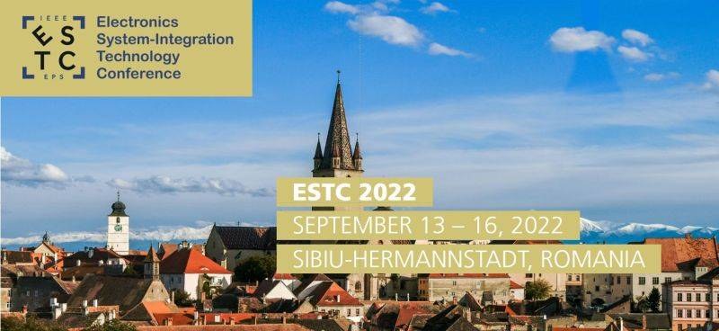
    The 9th Electronics System-Integration Technology Conference is taking place this year on September 13-16, 2022, in Sibiu, Romania.
    Veröffentlicht
    07. Juli 2022
    Lesezeit
    1 Minute
    Rubrik
    Semiconductor-packaging

    A variety of courses and workshops will be available, including topics on electronics manufacturing digitalization, component shortages, fan-out wafer level packaging, and additive printing. Special keynote presentations will also take place throughout this in-person event, covering information on heterogeneous technology, lithium-ion batteries, reliability testing and sustainability, CNF-MIM technology, flexible hybrid electronics and more.

    Participants, including scientists, engineers, and students, will all gather under one roof at this international forum to discuss the latest developments and future advances and research on microelectronics packaging. Welcome reception and social events throughout the 4-day event will further expand networking possibilities to talk with the experts of the electronics industry about global challenges, industrial trends and its solutions. Industrial tours will also be offered on the last day of the event, to give participants the chance to visit facilities and institutions, in order to experience it all firsthand.

    Since 2006, ESTC has been taking place every two years at different locations throughout Europe. This event continues to give the opportunity for academics and the industry to present, share, and discuss global trends and details regarding semiconductor packaging. This platform ensures a wide range of high-quality information is communicated through an interesting technical program to keep engagement and attention.


    Mehr aus Semiconductor-packaging

    Weitere aktuelle Artikel aus der Rubrik Semiconductor-packaging.

    Alle Semiconductor-packaging-Artikel
    Nanoscribe Expands Photoresin Portfolio for Micro-Optics Fabrication via Two-Photon PolymerizationFoto: Brecht Corbeel / Unsplash
    Semiconductor-packaging

    Nanoscribe Expands Photoresin Portfolio for Micro-Optics Fabrication via Two-Photon Polymerization

    11. November 2026

    Nanoscribe has detailed its range of photoresins engineered for Two-Photon Polymerization (2PP) and Two-Photon Grayscale Lithography (2GL), targeting high-precision micro-optics manufacturing on silicon, glass, and…

    Canon Launches FPA-6400ES6a KrF Lithography System with 400 Wafers-per-Hour ThroughputFoto: Canon Europe (semicon)
    Semiconductor-packaging

    Canon Launches FPA-6400ES6a KrF Lithography System with 400 Wafers-per-Hour Throughput

    10. November 2026

    Canon has announced the FPA-6400ES6a KrF scanner for semiconductor lithography, combining a throughput of 400 wafers per hour with industry-leading overlay accuracy of 4.0 nm and the ability to handle wafer warpage of…

    Fabmatics absorbs SCI business activities under unified brandFoto: Ludovico Ceroseis / Unsplash
    Semiconductor-packaging

    Fabmatics absorbs SCI business activities under unified brand

    6. November 2026

    Fabmatics has integrated the business activities of SCI under the Fabmatics brand, consolidating the acquired expertise within its semiconductor automation portfolio.

    Entegris and Kioxia Expand Partnership on Materials Innovation for Next-Gen 3D Flash MemoryFoto: Louis Reed / Unsplash
    Semiconductor-packaging

    Entegris and Kioxia Expand Partnership on Materials Innovation for Next-Gen 3D Flash Memory

    6. November 2026

    Entegris and Kioxia are deepening their strategic partnership to co-develop materials and process technologies for future BiCS FLASH 3D NAND architectures, using AI, digital-twin modelling and experimental validation at…

    ← Zurück zu Semiconductor-packagingZur Startseite

