
Zum Inhalt springen
EPP Europe
  • News
  • Products
  • Applications
  • Technology
  • Semiconductor
  • Inspection
  • Company News
  • Events
EPP Europe
  • Technology
  • Inspection (AOI/AXI)
  • Semiconductor Packaging
  • Company News
  • Products
  • Trade Shows & Events
    EPP Europe Newsletter
    The most important electronics-manufacturing news delivered to your inbox.

    Info

    • Impressum
    • Datenschutz
    • Barrierefreiheit
    • Datenschutzeinstellungen

    Kontakt zur Redaktion

    EPP EuropeKonradin Mediengruppe
    Ernst-Mey-Str. 8, 70771 Leinfelden-Echterdingen

    E-Mail: redaktion@konradin.de
    Folgen Sie uns
    EPP Europe
    © 2026 EPP Europe
    Startseite/News/Artikel
    3D & Systems Summit to spotlight hybrid bonding, chiplet design, sustainability
    Bildquelle nicht angegeben
    News

    3D & Systems Summit to spotlight hybrid bonding, chiplet design, sustainability

    Leading experts in 3D integration and systems for semiconductor manufacturing applications will gather at the annual SEMI 3D & Systems Summit, 12–14
    Veröffentlicht
    15. April 2024
    Lesezeit
    2 Minuten
    Rubrik
    News

    Heterogeneous Systems for the Intelligently Connected

    Themed Heterogeneous Systems for the Intelligently Connected Era, this year’s SEMI 3D & Systems Summit will feature a broader scope of topics including market trends, chiplet design, hybrid bonding, Co-Packaged Optics (CPO), high-bandwidth computing and environmental sustainability.

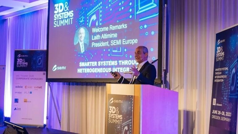
    “We look forward to hosting the most prominent names in 3D integration microelectronics manufacturing to showcase their latest products and technologies at the 3D & Systems Summit,” said Laith Altimime, President of SEMI Europe. “With advanced packaging innovations critical to enabling environmental sustainability while increasing chip performance, we look forward to hosting experts who will discuss the microelectronics industry’s work to explore more eco-friendly alternatives to conventional materials.”

    3D Summit sessions

    Session 1: Semiconductor Market Trends and European Impact

    Executive leaders will analyze the dynamic relationship between global semiconductor trends and the European landscape, highlighting the implications for Europe’s economic expansion and technological progress.

    Session 2: Chiplet System Architectures – Design and Technologies

    Industry experts will delve into dynamic chiplet design, emphasizing innovative approaches, emerging trends, optimization strategies, and packaging solutions that drive chiplet innovations.

    Session 3: Hybrid Bonding Technologies for Advanced 3D Integration

    Specialists will spotlight the latest advancements in hybrid bonding technologies, focusing on recent developments, novel techniques, and emerging applications. Speakers will highlight hybrid bonding’s transformative potential for enhancing semiconductor performance and overall functionality.

    Session 4: Manufacturing Innovation for 3D Integration

    Visionaries will showcase the newest hybrid bonding advancements, emphasizing their potential to enhance chip performance, efficiency, and functionality through recent innovations and emerging applications.

    Session 5: Co-Packaged Optics (CPO) – Innovations for High Bandwidth Computing

    Leaders will explore CPO as an advancement in integrated photonics, highlighting its cost-effectiveness, enhanced integration, and potential to improve performance in data transmission and processing systems.

    Session 6: Materials and Processes Supporting Environmental Sustainability

    Experts will spotlight semiconductor industry efforts to prioritize environmental sustainability through collaboration, innovation, and a continued commitment to exploring eco-friendly alternatives and reducing the industry’s environmental footprint.

    Global leaders to present

    3D & Systems Summit presenters include experts from these global leaders:

    • CARIAD
    • CEA-Leti
    • EPIC
    • EV Group
    • Fraunhofer IIS-EAS
    • Fraunhofer IZM-ASSID
    • imec
    • KLA Corporation
    • MKS-Atotech
    • NVIDIA
    • Silicon Saxony
    • SPTS Technologies Ltd., a KLA company
    • STMicroelectronics
    • TechSearch International, Inc.

    For more information, visit the 3D & Systems Summit 2024 website

    Mehr aus News

    Weitere aktuelle Artikel aus der Rubrik News.

    Alle News-Artikel
    Microtronic Takes on Distribution of iRaptor EYE Thermal Profiler in GermanyFoto: Laurens van der Drift / Unsplash
    News

    Microtronic Takes on Distribution of iRaptor EYE Thermal Profiler in Germany

    9. November 2026

    German distributor Microtronic has announced it will represent iRaptor LDA and its EYE thermal profiler in Germany. The Portuguese developer's system extends beyond conventional 2D time-temperature profiling by…

    Indium Corporation Presents Solder Materials Research at SMTAI 2026Foto: Indium Corporation
    News

    Indium Corporation Presents Solder Materials Research at SMTAI 2026

    29. Oktober 2026

    Indium Corporation is fielding five specialists at SMTA International 2026 to present new findings on solder paste rheology, BGA ball alloy selection for lower-temperature reflow, and the effect of print gap on paste…

    KYZEN to Present AQUANOX Aqueous Cleaning Chemistries at SMTA International 2026Foto: Vishnu Mohanan / Unsplash
    News

    KYZEN to Present AQUANOX Aqueous Cleaning Chemistries at SMTA International 2026

    16. Oktober 2026

    KYZEN will exhibit its AQUANOX line of aqueous electronics cleaning chemistries at SMTA International, October 27–29, 2026, highlighting prolonged bath life as a process efficiency and cost-reduction lever for…

    Fuji America and Cybord Partner to Integrate Visual AI Component Inspection into SMT LinesFoto: Cybord
    News

    Fuji America and Cybord Partner to Integrate Visual AI Component Inspection into SMT Lines

    29. August 2026

    Fuji America Corporation and Cybord have announced a strategic partnership to embed AI-powered component analytics directly into SMT production lines, enabling 100% real-time inspection of electronic components during…

    ← Zurück zu NewsZur Startseite


