
Zum Inhalt springen
EPP Europe
  • News
  • Products
  • Applications
  • Technology
  • Semiconductor
  • Inspection
  • Company News
  • Events
EPP Europe
  • Technology
  • Inspection (AOI/AXI)
  • Semiconductor Packaging
  • Company News
  • Products
  • Trade Shows & Events
    EPP Europe Newsletter
    The most important electronics-manufacturing news delivered to your inbox.

    Info

    • Impressum
    • Datenschutz
    • Barrierefreiheit
    • Datenschutzeinstellungen

    Kontakt zur Redaktion

    EPP EuropeKonradin Mediengruppe
    Ernst-Mey-Str. 8, 70771 Leinfelden-Echterdingen

    E-Mail: redaktion@konradin.de
    Folgen Sie uns
    EPP Europe
    © 2026 EPP Europe
    Startseite/Semiconductor-packaging/Artikel
    Global 200mm fabs to reach record high capacity by 2026, SEMI reports
    Bildquelle nicht angegeben
    Semiconductor-packaging

    Global 200mm fabs to reach record high capacity by 2026, SEMI reports

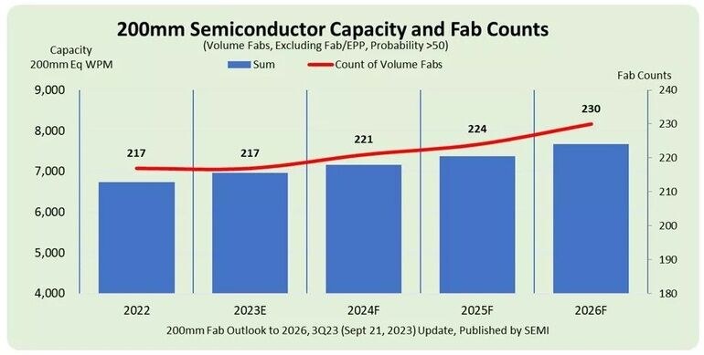
    Semiconductor manufacturers worldwide are projected to increase 200mm fab capacity by 14% from 2023 through 2026, adding 12 new 200mm volume fabs
    Veröffentlicht
    16. Oktober 2023
    Lesezeit
    2 Minuten
    Rubrik
    Semiconductor-packaging

    Power and compound semiconductors, which are vital for the consumer, automotive and industrial sectors, are the biggest drivers of 200mm investment. The development of powertrain inverters and charging stations for electric vehicles (EVs) in particular is expected to fuel increases in global 200mm wafer capacity as EV adoption continues to rise.

    “The global semiconductor industry’s ramp to record 200mm fab capacity highlights the bullish expectations for growth in the automotive market in particular,” said Ajit Manocha, SEMI President and CEO. “While automotive chip supply has stabilized, the increased chip content in EVs and the drive to reduce charging time is spurring capacity expansions.”

    Chip suppliers including Bosch, Fuji Electric, Infineon, Mitsubishi, Onsemi, Rohm, STMicroelectronics and Wolfspeed are accelerating their 200mm capacity projects to meet future demand.

    The SEMI 200mm Fab Outlook to 2026 report shows fab capacity for automotive and power semiconductors growing 34% from 2023 to 2026, with Microprocessor Unit/Microcontroller Unit (MPU/MCU) ranking second at 21%, followed by MEMS, Analog, and Foundry at 16%, 8%, and 8%, respectively.

    Accounting for most of the 200mm fab capacity are 80nm to 350nm technology nodes. Growth of 80nm to 130nm node capacity is forecast to expand by 10%, while 131nm to 350nm technology nodes are expected to register an 18% expansion from 2023 to 2026.

    Southeast Asia is projected to lead 200mm capacity growth with a 32% increase during the report period. China is expected to rank second with 22% growth. The biggest contributor to the 200mm capacity expansion, China is projected to reach more than 1.7 million wafers per month by 2026. Americas, Europe & Mideast, and Taiwan will follow at 14%, 11%, and 7% growth, respectively.

    In 2023, China is forecast to claim 22% share of 200mm fab capacity, while Japan is expected to account for 16% of total capacity, followed by Taiwan, Europe & Mideast, and America at 15%, 14%, and 14%, respectively.

    The SEMI 200mm Fab Outlook to 2026 report tracks 336 fabs and lines (from R&D and volume). The report includes 88 updates across 79 facilities and lines, including 12 new facilities since the previous update in March 2023.


    Mehr aus Semiconductor-packaging

    Weitere aktuelle Artikel aus der Rubrik Semiconductor-packaging.

    Alle Semiconductor-packaging-Artikel
    Kosmek Publishes Semiconductor Manufacturing Automation CatalogFoto: Kosmek (semicon)
    Semiconductor-packaging

    Kosmek Publishes Semiconductor Manufacturing Automation Catalog

    13. November 2026

    Kosmek has released an industrial automation catalog focused on semiconductor manufacturing, detailing pneumatic supports, robotic hand changers and locating components applicable across front-end and back-end…

    Nanoscribe Expands Photoresin Portfolio for Micro-Optics Fabrication via Two-Photon PolymerizationFoto: Brecht Corbeel / Unsplash
    Semiconductor-packaging

    Nanoscribe Expands Photoresin Portfolio for Micro-Optics Fabrication via Two-Photon Polymerization

    11. November 2026

    Nanoscribe has detailed its range of photoresins engineered for Two-Photon Polymerization (2PP) and Two-Photon Grayscale Lithography (2GL), targeting high-precision micro-optics manufacturing on silicon, glass, and…

    Canon Launches FPA-6400ES6a KrF Lithography System with 400 Wafers-per-Hour ThroughputFoto: Canon Europe (semicon)
    Semiconductor-packaging

    Canon Launches FPA-6400ES6a KrF Lithography System with 400 Wafers-per-Hour Throughput

    10. November 2026

    Canon has announced the FPA-6400ES6a KrF scanner for semiconductor lithography, combining a throughput of 400 wafers per hour with industry-leading overlay accuracy of 4.0 nm and the ability to handle wafer warpage of…

    Fabmatics absorbs SCI business activities under unified brandFoto: Ludovico Ceroseis / Unsplash
    Semiconductor-packaging

    Fabmatics absorbs SCI business activities under unified brand

    6. November 2026

    Fabmatics has integrated the business activities of SCI under the Fabmatics brand, consolidating the acquired expertise within its semiconductor automation portfolio.

    ← Zurück zu Semiconductor-packagingZur Startseite

