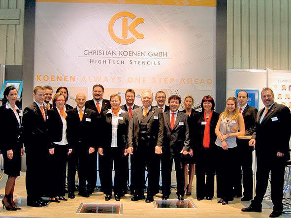
Koenen GmbH and Christian Koenen GmbH (the Koenen group) presented itself for the first time at the SMT/Hybrid/Packaging 2007. Since August 2006 both companies have concentrated on their respective core competence. Koenen has specialised in precision screens, and Christian Koenen in precision stencils. They develop, produce and distribute worldwide all types of precision screens and precision stencils for technical screen printing. With three plants and an office and production area of currently 5,500 sqm, the group secures the production location Germany and the future of medium-sized business. More than 100 employees at Ottobrunn near Munich are proud of the quality seal “Made in Germany”. The two owner-run companies draw their strength from the family roots and a rich tradition.
The re-orientation was met by positive response on the market. Their customers benefit from the common pool of experts. These are users with hands-on experience. They include a wide range of experts – from the electrical engineering technician to the engineer. The process support, which assists and trains the customers on site, is another strength of the group. Professionally well-founded and feasible overall solutions are thus achieved. Politicians and economists are delighted about the concentrated investment force. Jointly, the companies have increased their investment in research and development. The concentrated investment in new technologies secure quality already today, for example by a trade fair equipment pool valued at one million Euro. The frame cleaning that is free from residues and gentle on materials has become the quality standard for both companies. A joint application centre is to follow as a next step.
Isabella Koenen, Managing Partner of Koenen GmbH, and Christian Koenen, Managing Partner of Christian Koenen GmbH, agree: “Focussing on the respective strengths in the area of precision screens and precision stencils is a logical and consistent step. The cooperation as far as our experts, technologies, feasible problem solutions for our customers, research and development are concerned, is more than forward-looking. We thus secure quality and growth.”
Christian Koenen presented its further improved SMD step stencils. The SMD step stencils that are manufactured in a special procedure and intended for the application of different paste heights are one of the most innovative products of the company. Where the paste application in mixed assemblies can no longer be controlled to a sufficient degree by adapting the pad sizes, step stencils are used for an optimal adjustment of the solder paste volumes. With the novel patented procedure, it is possible to process the steps accurately with a precision of ± 3 μm over the entire surface. Different step heights or depths can thus be placed on the squeegee and/or the circuit board side.
In September 2006 Koenen GmbH started working on the research project “nanoSieb“ of the Federal Ministry of Education and Research. The overall goal of the project is to reduce the structure widths in screen printing. At the end of the 3-year project, conductor paths of 20 μm are to be realised in fine line print on ceramic circuit carriers, which can be produced industrially. The enterprise focuses primarily on the development of special screens. The further development and improvement of materials and processes during screen tensioning and screen structuring are of prior importance in this regard. The results to be achieved in the project are to facilitate the use of screen printing technology for new or alternative applications.
In addition, SMD stencils, stencils for wafer and LTCC technology, fast-ening systems, the SMDS special cleaner series “cleanteCK”, washing systems, precision screens in base line, fine line, ultra fine line, nano line, trampoline screens and hotscreen technology, as well as other interesting products were presented.
EPP Europe 409
Share:


