The voiding in new generation solder joints will probably not be the worry in terms of joint reliability as may initially have been thought. That is the encouraging outcome of a comprehensive DTI-supported study carried out by the National Physical Laboratory and nine industrial partners.
As the date for the ban on lead in electronics assemblies rapidly approaches (July 2006), all is not yet plain sailing for users of lead-free soldering systems in this transition period. The industry is in general agreement that the preferred solder replacements are based on tin-silver-copper (SAC) alloys, which have melting points of 217 ºC and above.
However, there are still a number of concerns that the industry must allay before full confidence in the new technology is achieved. Among them is the perception that lead-free soldering would be prone to excessive voiding, a view consistent with some of the known causes of voiding, such as faster ramp rates and higher peak profile temperatures. Indeed, the 30–35 ºC increase in melting point from that of the conventional SnPb solder necessitates a similar increase in processing temperatures for both reflow and wave-soldering, and there were worries that this might result in increased levels of voiding which in turn would degrade joint and assembly reliability.
There is a perceived link between voiding and a reduction in reliability. Ultimately at high voiding levels, the remnant material cross section along the crack path is insufficient and ensuing failure will be more rapid. But in studies where voiding levels of up to 24 % in BGAs were characterised, no reduction in reliability was observed in joints soldered with SnPb alloy. The industry has never the less adopted a cautious approach to voiding, and has adopted a strong preference for low or 0 % voiding.
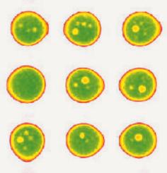
Currently, there is a paucity of data for voiding and its effect on reliability for joints assembled using lead-free solders, surprising in view of industry’s current surge in legislation-driven change to lead-free technologies. But the NPL work has gone some way to redress this balance, and generated data, which has dispelled the concern that excessive voiding would be associated with lead-free soldering. In particular, the work has demonstrated that average-voiding levels in lead-free solder joints can be kept well below the IPC specified maximum, a fact welcomed by industry. The programme of the National Physics Laboratory (NPL) was carried out in two phases. First, test boards, containing ceramic chip resistors, SOICs and PBGAs, were assembled. And that under a range of reflow conditions in order to identify the processing required to produce three widely different levels of voiding.
Encouragingly, the results showed that for a wide range of lead-free soldering conditions, it was very difficult to generate the high levels of voiding previously achievable with similar SnPb soldering profiles. The soldering conditions which have been used are seven solder pastes from three manufacturers in water-based pastes, three reflow profiles and with non standard excessively fast ramp rates, and high peak temperatures. Moreover, the low voiding levels were similarly encountered across the whole range of lead-free solder technologies studied. They were all below the levels permitted in IPC A610 revision D (25 % by area).
The second phase examined the influence of the voiding observed in the SAC soldered assemblies, on the integrity of the joints. Further assemblies which were prepared having the three different voiding levels, were subjected to thermal cycling (between –55 ºC and +125 ºC for 2000 cycles). The joints’ integrity was monitored using visual, electrical continuity, and shear strength techniques. Despite the joints of BGA components having voiding levels up to 13 % by area (i.e. 4% higher than those stipulated for class 3 of the more stringent IPC 7095A Design and Assembly Process Implementation for BGAs), there was no adverse effect on the joints’ reliability. Moreover, there was no effect on the shear strength of the joints of chip resistors having the same high levels of voiding.
Supporting evidence was obtained by subjecting joints having up to 13 % voiding, to extensive thermal cycling (–55 to +125 ºC; 2000 cycles). As monitored using electrical resistance, shear strength, or shear strength deterioration during thermal cycling, there were no differences in reliability of the joints. The results clearly suggest that if the IPC maximum voiding levels are adhered to, there should be no adverse effect from voiding on the reliability of lead-free solder joints.
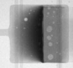
We gratefully acknowledge the support of Dage in providing X-ray images. This work was supported by the DTI and others of the NPL IAG group. A full version of the work is available at http://www.npl.co.uk/ei/research/mpp52.html
Chris Hunt, Martin Wickham
Share:


