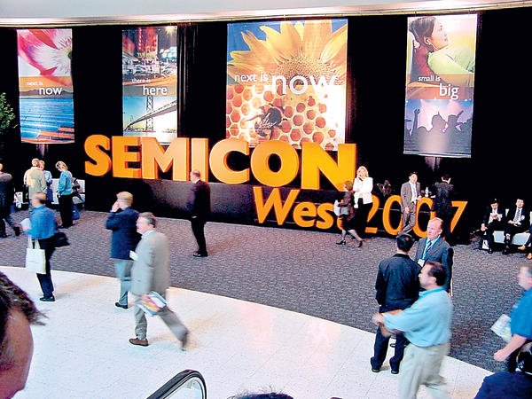
With its 2007 edition, SEMI is proud to announce that its flagship event “Semicon West” is back on course as the premier venue for semiconductor manufacturing equipment and materials vendors around the world. A plus of 12 % in attendance numbers – 14,238 of them counting as verified visitors, excluding an about equal number of exhibitor staffers – looks and feels good after last year’s precipitous drop. About 1200 “exhibiting companies” took part in San Francisco’s roomy Moscone Convention Center, offering enough space for the equipment industry to get together, talk shop and present its product portfolios – together with discussing the future in view of costly investments in advancing fabs and equipment.
A total of 500 new product introductions as SEMI has officially counted them were also part of the show – as if that would be of any significance in today’s instantly networked information communities as the worldwide semiconductor industry and its suppliers is, with news information flowing top-down at their own pace and competitive advantage of the market leaders. And the next major event, Semicon Europa, at its newly found home in Stuttgart, Germany, taking place from 9 to 11 October 2007, will be already around the corner when this report from Semicon West is published in EPP Europe.
So, what was the agenda of Semicon West 2007? The usual pace of innovation which the industry more or less voluntarily has agreed to meet along the lockstep of Moore’s Law. (If only Moore’s Law by name and out of respect for one of the last living legends of the original Silicon Valley, California.)
It’s a multi-dimensional advance of the semiconductor technologies by now as the ISMI (International Sematech Manufacturing Initiative) and the ITRS Roadmap committees hammered into the heads of technologist again at Semicon West 2007. It’s “More than Moore” now: Traditional geometry scaling complemented by equivalent scaling for CMOS circuitry, now at the 45 nm half pitch node and transiting to 32 nm in the coming months, and looking out scared to 22 nm and beyond, whereas 65 nm is a thing of mainstream routine.
The other evolutionary dimension now is diversifying the device roadmap and production processes into HV power, passives, sensors/actuators, biochips, and the like. No dearth of exotic concepts here as time progresses. And, of course, proud mainstay of European research and design achievements, there is the continuing push into SoC and SiP, with the aim of creating “higher-value systems” – something “beyond CMOS.” This is self-evident since the industry now is unit and volume driven, not margin driven, due to its dependence on its main customers: The consumer electronics industries with their relentless demand for lower cost and higher value.
The mid-year economic outlook of the equipment and materials industries, not yet impacted by the U.S. mushrooming real-estate and hedge-fund crises is good but turning into a somewhat muddy situation. The North-American book-to-bill ratios as calculated by SEMI, are down from a splendid 0.98 last February to a more modest 0.88 in July (Tables 1 and 2). But there was a continuous climb in absolute numbers until June when billings and bookings alike began to fall, with bookings falling a bit faster then billings. “The declining book-to-bill rate is based on lower order levels for new semiconductor manufacturing equipment,” says experienced industry veteran Stanley Myers, President and CEO of SEMI. “They are at levels last seen in November 2006.”
So, according to SEMI, the equipment markets are to take a breather this year – if on a high level – with growth scheduled to be just 1 %. In other words: Stagnation. Last year, the market grew by 23 %. In 2008, a steeper rise is supposed to return: At 6.5 %, followed by 4.4 % in 2009, Myers predicted. Let’s wait and see how it turns out.
Looking at the constituting segments of the industry, there are different developments. The front end, with wafer processing, still is expanding in 2007, by 4 % (to $29.8 billion). But testing is coming down by 8 % (to $5.9 bn). Assembly and packaging will be basically flat at a total of $2.5 bn. Regionally growth will be centered in Taiwan this year, with an accelerated increase of 20 %. China is also poised to grow but with lesser impact on overall industry performance because the outlays there are still comparably small despite huge investments in fab capacity. Japan, the U.S. and Europe all are destined to loose in volume this year.
Quite different, on a more positive note, but driven by the same dynamics, is the materials segment. It is supposed to grow this year by 10 %, and another 9 % in 2008. Why? Because of the strong unit and volume boom in semiconductors is consuming record amounts of silicon (a scarce resource these days as the photovoltaic panel manufacturers have come to accept). Packaging materials alone will reach $16.6 bn this year – an increase of 9 % – most of them flowing to Japan and Taiwan. “Semiconductor unit growth, the 300 mm ramp and the transition to flip chip”, says Dan Tracy of SEMI, “are driving the revenue growth in the semiconductor market”. Not without a hitch: Higher raw material prices are a challenge to suppliers and customers alike.
Consequently, investment versus profitability was the key topic at Semicon West 2007 – as it has been every year. But R&D costs are proportionally rising ever faster than profits, as Steve Longoria of IBM, East Fishkill, said in a presentation. This will lead to an even more massive industrywide collaboration and cooperation virtually along the entire value chain. No wonder: The investment cost for new fabs is rising out of sight, Longoria said. The transition to 45 nm upon us, may involve a total bill of $2.4 bn in fab expenses.
Fab productivity was one of the buzzwords to be heard in the product announcements around the show floor and in the conference sessions – in the sense to slow down the generational changes such as the transition to 450 mm wafers, or in the ways to accelerate wafer processing by parallel work flows. Or the migration to smaller batches, even single-wafer processing. “300 mm Prime” is such a concept of productivity enhancement by drawing out new investment to a later day. “We believe that huge benefits can be attained by improving 300 mm fab productivity”, Myers says.
On to the technological issues present at Semicon West 2007, as they pertain to the back-end segments, namely test and packaging. The “Test summit”, a new feature of the show, was supposed to discuss new test technologies and strategies. This year, Advantest, Credence, Nextest, Teradyne and Verigy all joined the stage to get to the transition to 45 nm CMOS half pitch by providing the appropriate automated equipment.
The key drivers for enhancing test strategies, says Roger Barth of the ITRS Test Working Group, are the current and future device trends, such as higher interface bandwidths between devices. Then: Increases of integration density such as brought on by SoC, SiP, MCP and 3D in general. And finally: The integration of emerging CMOS technologies with vastly more complex packages and their quickly developing characteristics.
Increasing test complexity – more cores, more transistors, more bits and higher speeds – is also a challenge imposed by device customization, distributed test strategies out of cost considerations and the uncomfortable issues of “adaptive test.” Economics play into testing by approaching the physical limits of test parallelism and managing test data volumes. Overall, it’s the historical conflict between the cost of test and the cost of quality.
Another development arriving with continuing device scaling is the fact of systemic defect mechanisms in devices – not just the hard defects caused by design flaws and manufacturing deficiencies. Among these are finite dopant distribution causing erratic, non-deterministic functional behavior, and the like – where no clever test strategy can go. Additionally, unresolved tester inaccuracies in terms of timing, voltage, temperature control, etc., are playing an ever wider role. The way out: The continuing economic scaling of test and the principle of “yield learning through test”. Just think of the growing complexity of future SiPs – and the test issues they are going to raise.
Well attended was the ITRS presentation on interconnect, given by Christopher Case of Linde. It’s difficult enough to meet the challenges of scaled metal-dielectric interconnects, he pointed out. It’s all the more challenging to meet the requirements of equivalent device scaling. Besides 3D there is talk of optical wiring and other non-traditional materials. Adding functional diversity of circuitry by combining mixed technologies brings together materials such as Si, GaAs and HgCdTe – their properties all to be compatible with traditional CMOS materials and processing steps. Emerging interconnect types will use optics (waveguides, emitters, free space, modulators, and the likes, as well as RF/microwaves or Terahertz photonics – leave alone the really “radical solutions” such as nanowires, molecules and spintronics, even quantum wave functions.
Back to Earth, into packaging: In the light of three-dimensional device scaling, current packaging methods can’t keep up. It now is the limiting factor in system cost and performance. Up to now, wafer thinning, wafer-level packaging, new materials have done the trick – all driven by the “consumeration of electronics.” From now on, packaging materials will have to change (or have already changed) due to performance considerations and/or environmental regulatory impositions. This pertains to everything: Bonding, molding, underfill, thermal interfaces, die attach, substrates and solder.
Especially stacked die SiPs at wafer level will bring a host of new challenges, in terms of signal and power integrity and their shielding, once they have grown to nowadays unseen complexities by 2010. At the 14 nm device node there may be power densities of > 100 W/cm² involved. Heat removal, on the other side, requires greater component volumes equaling longer wires, higher latency, and more. Thermo-fluidic cooling may be required. All this is, as Semicon West 2007 proved, still in an “early definition phase.” But nevertheless the issues are pressing. (Werner Schulz)
EPP Europe 413
Share:


