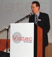
In March 2006 Vistec Electron Beam GmbH (previously Leica Microsystems Lithography GmbH) celebrated its 10th anniversary. Founded in 1996 as an independent company within the Leica Semiconductor Equipment Division, Vistec is a manufacturer of electron beam lithography systems used in microchip production, for integrated optics, and for academic and industrial research.
Along with the 10th birthday celebrations, Leica Microsystems Lithography GmbH also has a new name: Vistec Electron Beam GmbH, the result of the acquisition of Leica’s semiconductor activities by Golden Gate Capital, a investment company based in San Francisco (USA). The Jena, Germany facility is a business unit of Vistec Semiconductor Systems, which has over 500 employees around the world.
Electron beam lithography systems have been produced in Jena since the late 1960s, first as part of Carl Zeiss Jena, then, after the collapse of the GDR, as part of Jenoptik, and in 1996 as a division of Leica Microsystems. The new name is a combination of the words “visionary” and “technologies” and outlines the company goals – the development of new and forward-looking technologies.
With the development of the variable-shaped beam and numerous key patents for electron beam lithography, the company is no stranger to innovation. Vistec is the world’s first manufacturer to offer an electron beam lithography system that enables complete processing of 300 mm substrates. Today, 13 of these “stage systems” are in use at research and commercial sites around the world. Especially the ability to completely structure a 300 mm silicon wafer assured the company a leading role in Electron Beam Direct Writing (EBDW).
As part of a European MEDEA+ research project (financed by the German Federal Ministry for Education and Research) and cooperating with European semiconductor manufacturers, Vistec succeeded in developing a market-ready mask-free lithography solution.
In addition to an optimized “single beam process”, the company is participating in another European cooperative project to launch a highly innovative and completely new concept – a lithography process that uses massively parallel electron beams to structure masks or wafers.
EPP EUROPE 407
Share:


