Although many have predicted the demise of through-hole components, they are alive and well with tens of billions parts assembled each year. In many cases, these components are manufactured using wave soldering. However, in many mixed product technology board assemblies (i.e. SMDs – surface mount devices – and through-hole parts on the same board), it makes sense to consider assembling the through-hole elements with the pin-in-paste (PIP) process. For the advancement of this procedure, solder preforms in the Solder Fortification techniques can be used. In some applications, soldering defects were reduced by 95 % after implementing the preforms.
Carol Gowans, Paul Socha, Ronald C. Lasky, Ph.D., P.E., Indium Corporation, Clinton, NY, USA
The soldering technology pin-in-paste has been successfully used for several decades now. However, in many cases it is not possible to print enough solder paste to obtain acceptable solder joints for this technology. In addition to this “solder starved” condition, the large quantity of solder paste used to form the through-hole joints can result in excess residual flux supplied with the paste. This residual flux may lead to difficulties in in-circuit testing (ICT) of the board assemblies, and also rise potential concerns in regard to surface insulation resistance issues.
In light of the need to overcome these manufacturing problems, solder preforms have been developed. These slugs of solder typically come in the same sizes as 0402, 0201, 0603, and 0805 passive parts. The solder preforms are set down by the already existing component placement machines onto the before stencil-printed solder deposit. This additional solder assures that an adequate solder joint is formed with a minimum of solder paste and its residual flux.
Although PIP was an early application of solder preforms, more recently other “solder starved” applications have emerged such as radio frequency (RF) shields for PCB circuitry and connectors. In addition, the use of ultra-thin stencils in the assembly of miniaturized components can result in some other components being solder starved and, hence are candidates for solder performs. So let’s have a look at the design and assembly techniques for using of preforms in the main Solder Fortification application areas. Several successful implementations have already been provided. In some of these applications, defects were reduced by 95 % after employing solder preforms.
The pin-in-paste process
Through-hole technology still remains important in all kinds of state-of-the-art electronics. There are several reasons for this fact; one being that some components or connectors might only be available in through-hole technology, but more likely the mechanical strength of more solid through-hole connections is critical for long-term reliability in many applications.
As an example, a laptop PC usually has multiple USB, power, video, audio, and internet connectors. Many of these connectors need the strength of through-hole connectivity to withstand the multiple plugging and unplugging in their service life. Often these connectors are few in number and a full wave solder process to assemble them may not make economic sense. In such situations, as an alternative to the standard wave soldering, selective wave soldering may be an appropriate choice, or perhaps the pin-in-paste (PIP) process. The pin-in-paste process involves printing solder paste near or over the through-hole object. The through-hole component is placed and reflow soldered with the surface mount devices (SMDs). The development of an effective PIP process is discussed in references1) and2). PIP is usually performed with no-clean solder paste.
In many applications, PIP has several challenges. One being that so much no-clean solder paste has to be used to obtain an effective solder joint, that excessive residual flux can make electrical in-circuit testing (ICT) difficult. Another challenge of the PIP process is solder starvation which occurs because it is often not possible to print enough paste to form a complete solder joint. Even if a solder joint of this nature passes the procedures of the standard ANSI/J-STD-001C, many manufacturers and their customers would be dissatisfied with the quality of and potential reliability issues with such solder joints. The use of solder preforms to support the PIP process can mitigate both of these problems.
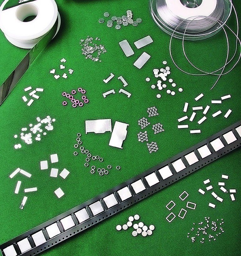
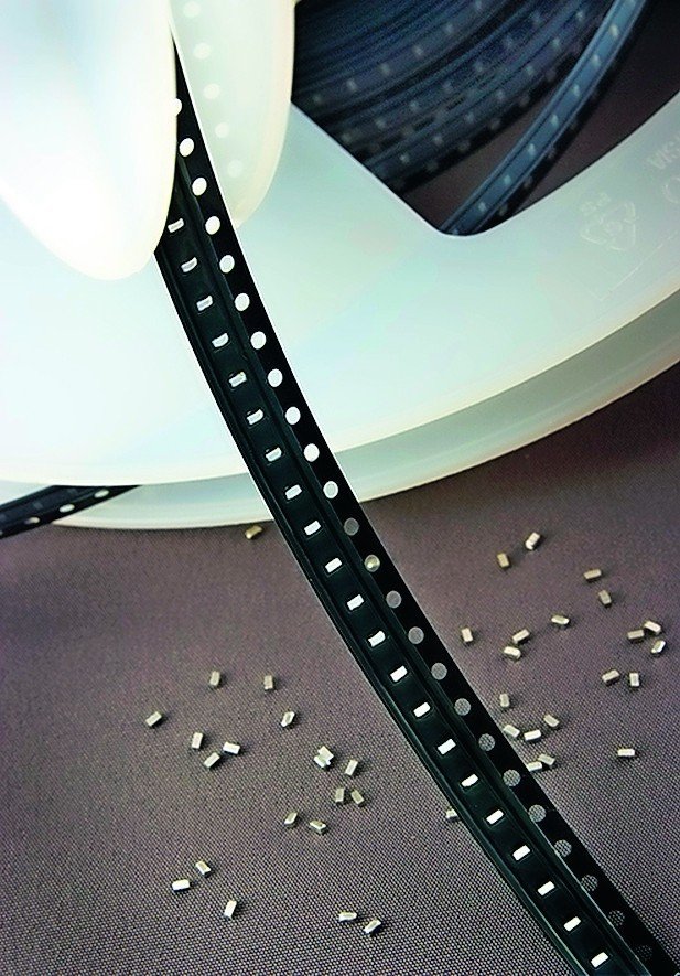
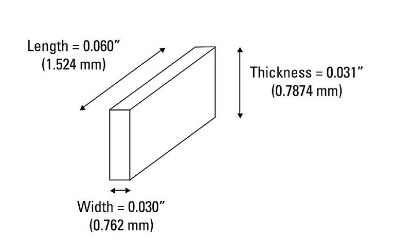
Solder preforms are stamped from rolled solder ribbon to the desired XY dimensions. Preforms are available in numerous shapes, sizes and alloys and are specifically designed to deliver an exact quantity of solder to a desired location. Typically solder preforms to support the PIP process are rectangular in shape and are the size of common passive components (e. g. 0201, 0402, 0603, etc.) so that they can be put in position by component placement machines. These preforms come in tape & reel feeder packaging. The solder preform process for through-hole connectors on mixed-technology boards utilizes current equipment and process expertise. A typical example follows:
Step 1: Solder paste is printed at the site of the connector pin. The solder paste deposit may be an overprint to provide a wicking path for the preform. For example, a preform can be placed in the overprint portion and during reflow the preform solder will wick to the pin. Additional flux is not required because sufficient fluxing activity is available in the solder paste.
Step 2: Preforms are placed in the solder paste using automated placement equipment. The preform shape may be a washer or a 0603 segment.
To achieve excellent results with the solder preform plus solder paste solution, the paste is printed and the preform is located on the paste with a component placement machine. The benefits were:
- Full barrel fill that is easily inspected
- No loss of throughput
- Elimination of step stencil with reduced defects at fine-pitch devices
- Reduction of overprint, which eliminated solder beads and balls
- Increased flexibility for future designs
This process achieved good hole-fill and ease of inspection of the solder joints. While PIP was an early adaptor of preforms, more recent Solder Fortification applications may actually be more popular. Two of these applications follow.
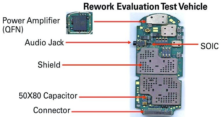
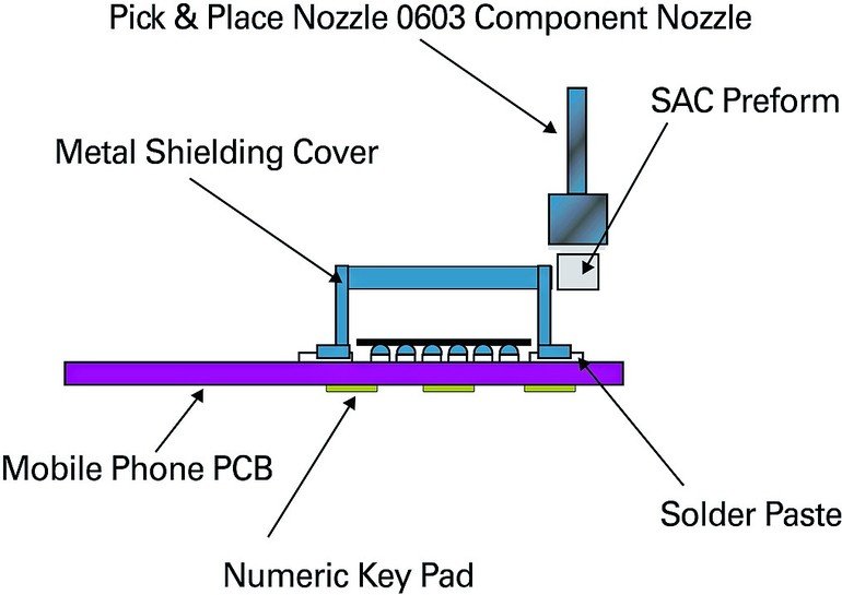
Grounding of mobile phone shields
Most of us probably don’t think about it, but a mobile phone is really a radio. As a sophisticated radio, it is very susceptible to stray electromagnetic (EM) waves or electrostatic discharge (ESD). These threats could potentially cause serious malfunctions. In light of this concern, mobile phone designers encase the most EM/ESD sensitive components in the mobile phones in Faraday shields. To assemble these shields to the board circuit, solder paste is printed onto the receiving pads and the metal shields are attached during the normal reflow soldering procedure. Due to the miniaturization and increased functionality of mobile phones, in some designs it is difficult to print enough solder paste to electrically connect the shield to the pad on the board assembly so that the shield can successfully perform its ESD and EM protection duties. Solder preforms were proposed as a potential solution to such solder starved conditions. In these processes, the component placement machine puts the preforms in position.
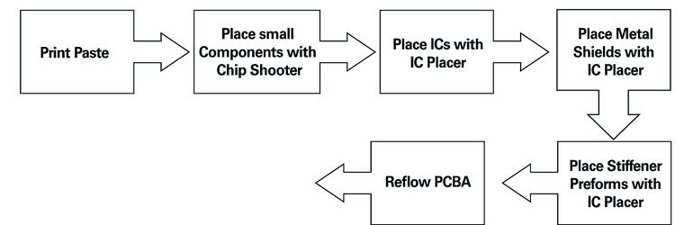
The SAC (tin-argentum-copper) preform is typically the size of an 0603 passive component. The volume of this preform should be calculated to deliver the needed amount of solder. Tape & reel feeder packing is typically used in this application for the preforms. After the solder paste is printed, a chip shooter places the tiny passives and small components. An component placer puts the ICs in place and later the shields. The solder preforms are then arranged by the IC placer. After these steps, the PCBA goes into the reflow oven.
It is possible, but not likely, that the placement of the preforms could slow the IC placer down. These types of applications have been implemented with high yields and reliability. In conclusion, solder preforms enable a low cost, reliable solution to solder starvation in Faraday shield assembly for mobile phones. In addition, the process is part of the in-line electronics board assembly and the final result is not visible to the end user.
Capacitor terminal applications
Terminals of large capacitors can also experience solder starvation. In one such application, 0603 size preforms were placed near the capacitor terminals. In this application, the number of solder-starved related defects was reduced by 95 % after using preforms.
Conclusion
Solder preforms can be an economical way to solve solder starved conditions in various types of SMT (surface mount technology) assembly applications. It is always best to consult with the technical support team at your solder supplier to be sure that the correct solder, solder form, and flux best suit your application.
SMT Hybrid Packaging, Booth 4-321
Share:


