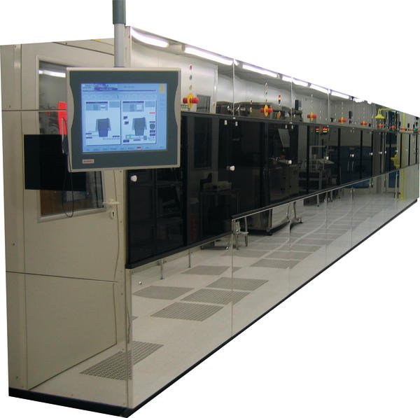
Pac Tech – Packaging Technologies GmbH announces that it has sold their latest PacLine 300 A50 system for electroless deposition of Ni, Pd and Au on advanced semiconductors to Diodes Incorporated in Plano, Texas. The system will be installed at Diodes wafer fabrication facility in Kansas City, Missouri. The system is a fully automated, self-contained, mass-production system capable of processing up to 150 wafers per hour and up to 600,000 8-inch wafers per year with full robotic handling of wafer carriers. The system is part of a turnkey process technology transfer, including the company’s proprietary process know-how and unique chemical product line. The state-of-the-art plating line will be equipped with fully automated chemical delivery unit (CDU) and will use a SECS GEM interface to communicate with the facility host system. As every Pac Tech equipment the design, hardware and software are conform to SEMI S2/S8/S14 standards. The system provides fully automatic bath controls, including automatic titration, temperature and flow control as well as pH measurements and replenishment. The electroless Ni and Pd process technology will enable Diodes to utilize high volume production capability at low processing cost due to parallel wafer processing for their packaging needs. One of the additional advantages of electroless plating is the absence of any tooling and sequential wafer processing such as lithography and sputtering. In general ENIG and ENEPIG metallizations are compatible with a variety of applications, e.g. UBM for WLCSP and flip-chip, frontside metallization for Power MOSFET for clip attach soldering and OPM for Cu and Au wire-bonding. It is compatible with all flip-chip or WLCSP assembly processes. Dr. Thorsten Teutsch, President of Pac Tech USA says, ”It is exciting to see that Pac Tech’s low cost technologies automated equipment lines are assisting to keep manufacturing jobs secured in the US.”
Share:


