Apart from the layout and housing design, the characteristics of the ICs used play a key role for the EMC characteristics of devices. Reducing the size of the structure, operating voltages and operating points makes the ICs much more sensitive. If one approaches or even surpasses the 100 nm limit, the immunity compared to earlier ICs is reduced, a trend that is reflected in the device behaviour. It is important that users of ICs are able to compare various types of IC on the basis of their EMC parameters. This enables the choice of the best IC, and means that the layout design and the device can be aligned to the IC’s EMC parameters.
Gunter Langer, Langer EMV-Technik GmbH
For manufacturers of ICs, good EMC characteristics for their products mean advantages over their competitors. The objective is thus to determine those parameters which are decisive for EMC immunity and emissions and allow engineers to draw conclusions for chip design.
Currently popular test methods for ICs
It is nowadays common to quote a value of one to several kV in specifications as the ESD strength of electronic components (ICs, transistors) with reference to the human body model. With the human body model (HBM), a capacitor (100 pF) is charged with a test voltage and discharged on the device under test via 1500 ohm. The HBM is described in the standards MIL-STD-883G and in IEC 801–2. The machine model (MM) is a further test model that works according to the same principle.
Both models are only used to validate the immunity to destruction of the IC when handling the component during its production, packaging, transport and assembly. During MM or HBM tests, the test object is never connected to a voltage, i.e. it is not in operation.
The specified ESD strengths according to the human body model do not relate to the ESD behaviour during operation. In fact, the protective mechanisms designed for the human body model (that do not take into account malfunctions during operation) may even cause faults or failures of the IC during a functional disturbance test.
Work is currently being carried out on EMC standards, test methods and limit values for ICs.
The requirements in terms of the EMC of devices (resources and equipment) are already defined in standards, test methods and limit values. The devices are subjected to an ESD and burst test (IEC standard 61000–4–2/61000–4–4), with test voltages in the kV range.
The ICs and other semiconductors used in the device are ultimately the causes of interference emissions and a lack of immunity.
The interference emitted by ICs can be measured at their interfaces and evaluated and defined on the basis of these measurements.
ICs have a low interference immunity with immunity levels in the volt range.
The pulse voltages introduced on the outside of the device during standard tests are attenuated on their way to the IC. A few kV outside the device are reduced to voltages of around 1 … 100 V at the IC pin. These voltages can exceed the immunity levels of the ICs. This means that compared to the device test, the test voltages for ICs have to be in the range of 1 to several hundred volts and not in the kV range. A higher test voltage is only required in a few exceptions (special devices).
New IC test system
The IC test system can be used to analyse the behaviour of ICs under the selective influence of (conducted and radiated) disturbances and/or respective emissions. The insights gained from this analysis help semiconductor manufacturers optimise ICs and IC users overcome weak points in their electronic modules. The test IC is tested in use.
The IC test system lets the user of ICs:
- identify EMC problems in the device on the IC level
- select ICs on the basis of the gained insights and
- optimise the circuit and/or layout design to the EMV parameters of ICs.
The IC test system lets the manufacturer of ICs:
- measure and check the immunity of/emissions from ICs
- identify the causes of interference and
- optimise the ICs
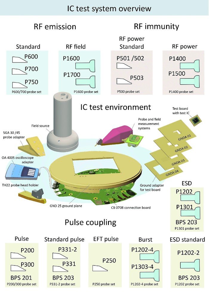
Different probe sets are needed to determine the various EMC parameters. The probe set can be selected by the user depending on the field of use (incl. RF, EFT, ESD, DPI, emissions 1 ohm method…).
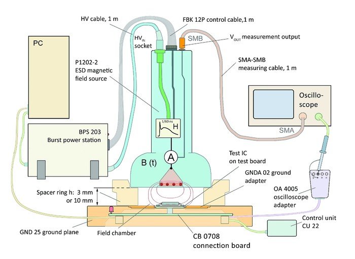
The ICE1 IC test environment is required as an optimum test environment for the probe sets:
- a test board for the test IC which provides a uniform interface between the test IC and test system
- a CB 0708 connection board which is used to trigger the test IC
- a GND25 ground plane which provides a uniform reference potential
In addition, external equipment may be necessary depending on the probe set and the respective job:
- a disturbance generator (e.g. EFT/burst)
- an oscilloscope
- a spectrum analyzer
- a PC
- a power amplifier
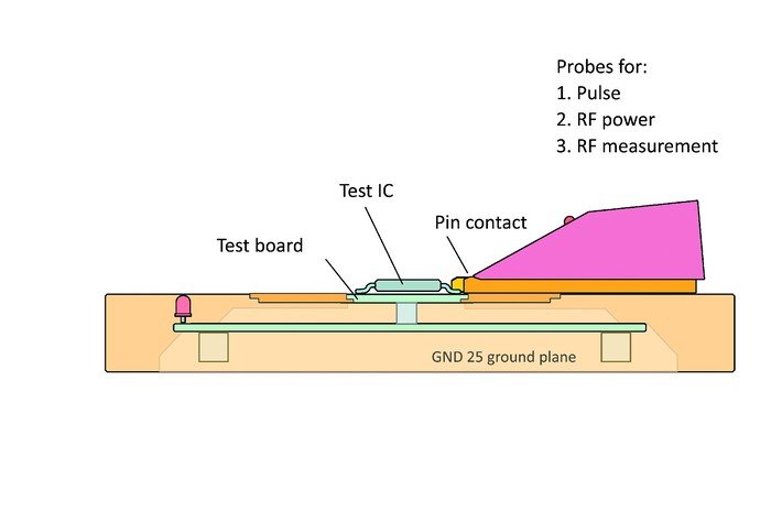
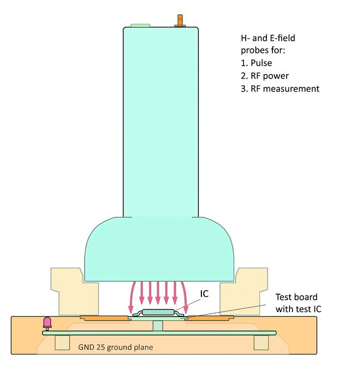
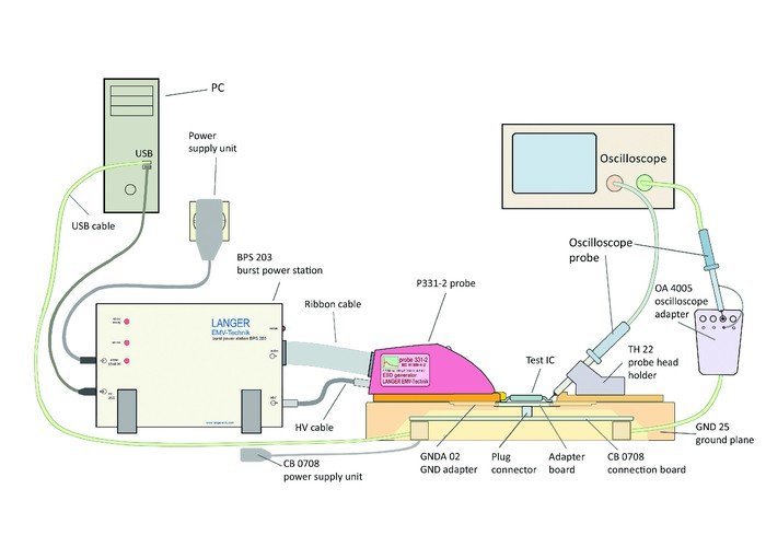
The IC under test is located on a test board in the test set-up. Filtered connections link the test board to the CB 0708 connection board located below this which connects the test IC to the PC. The IC can be controlled and monitored with the enclosed software. The connection board is integrated in the ground plane which forms a fixed ground reference system for the test. The probes from the probe set are placed onto the ground plane and used to inject disturbances into the test IC through conductive or capacitive/inductive coupling or to measure its emissions. Depending on the respective type, the probe set is supplied and controlled via an external disturbance generator (RF, EFT/burst), a spectrum analyser or the burst power station (BPS) from Langer-EMV.
The burst power station is included as an accessory with certain probe sets. The probe’s pulse voltage, pulse frequency and polarity can be modified with the enclosed BPS-Client control software.
EMC parameters for ICs
Each IC has characteristic immunity levels with regard to conducted and radiated interference. These are its EMC parameters. The IC pins have conducted immunity levels which can be measured with corresponding probes from the probe sets.
The IC as a whole has radiated immunity levels. Disturbance fields can affect the IC from the outside and exceed these levels of immunity to magnetic fields and electric fields. These immunity levels are independent of each other. Probes that generate suitable and defined fields are needed to determine the field immunity levels.
In addition, the conducted interference emission of an IC can be measured via the pins and the radiated (electric and magnetic near-field) emission via the IC housing. The measured curves are the EMC parameters by which the ICs can be analysed.
The IC under test is located on a test board in the test set-up. Filtered connections link the test board to the connection board located below this which connects the test IC to the PC. The IC can be controlled and monitored with the enclosed software. The connection board is located on the underside of the ground plane which forms a fixed ground reference system for the measurement. The probes are placed onto the ground plane and used to inject disturbances into the test IC through conductive or capacitive/inductive coupling or to measure its emissions. The measurement connection is made via the probe’s pin contact to the tested pin of the test IC. This small-scale set-up and the continuous ground layer ensure that measurements can also be carried out in the GHz range.
Definition of the test method
The EMC immunity and emission mechanisms active in the devices have to be analysed. The test methods for all interfering variables (RF, ESD, EFT, emission, RF emission…) are derived from this analysis.
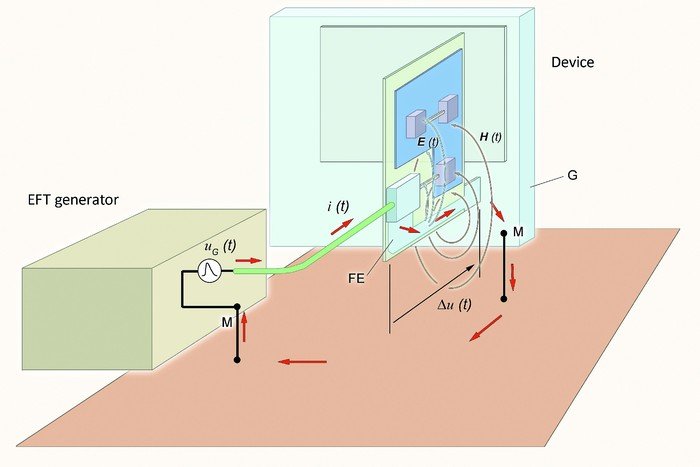
Interference immunity
The test methods for devices generate electric and magnetic fields in the device under test. These fields affect the networks of the printed circuit board that lead to the IC as well as the IC housing. The fields that act on the networks generate currents and voltages in these which affect the connected IC.
Test generators for ICs have to generally simulate these electrical and magnetic parameters. Figure 6 shows the basic set-up of a burst or ESD test bench. The test pulse injected into the device under test uG(t) generates a current pulse i(t) that flows through the device. This leads to a voltage drop Du(t) in the device. This voltage drop Du(t) produces the electric field strength E(t) in the device. The current i(t) produces the pulsed magnetic field H(t) in the device. These fields have an indirect effect on the externally connected conductor tracks (conducted) on the IC or directly on the IC housing (radiated).
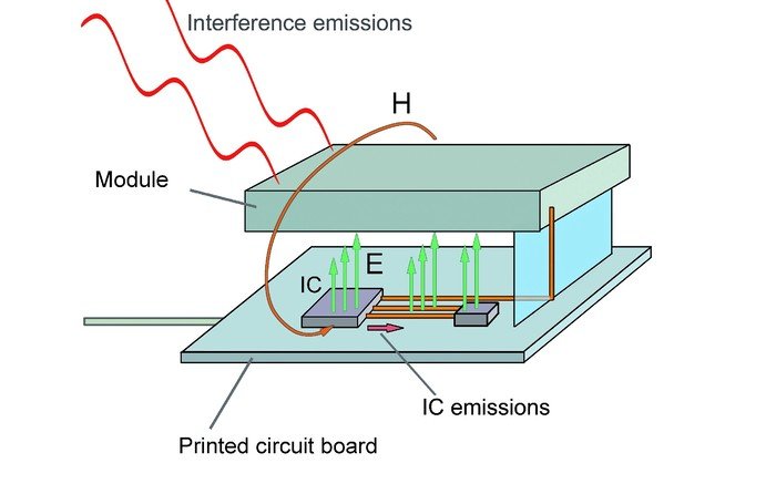
Interference emissions
Switched-mode ICs generate internal RF currents and voltages. These in turn generate electric or magnetic RF fields that escape directly from the IC housing. Furthermore, the RF voltages and currents may be transmitted to the IC pins and thus to networks outside the IC on the printed circuit board where they generate electric and/or magnetic RF fields. The electric field E is generated by the IC and the external network of the IC in Figure 7. The electric field couples across to the neighbouring component and stimulates this to emit interference. The EMC parameters of the IC in this case are the strength of the electric field emitted by the IC and the electrical parameters current and voltage (IC emission) with which the networks outside the IC are stimulated.
The parameters electric field, magnetic field of the IC housing and RF current and voltage of the IC pins have to be measured with suitable systems (probe sets). These are the characteristics of the IC.
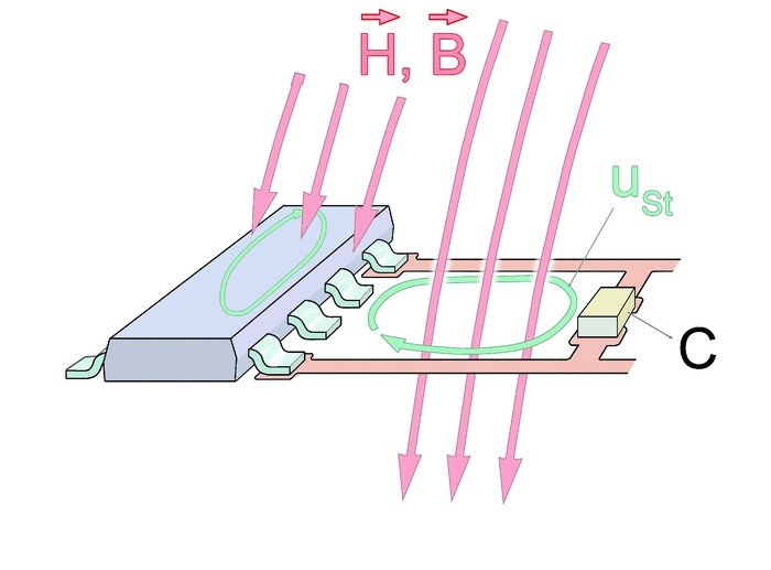
Magnetic/inductive coupling
The pulsed disturbance current flowing through a board generates pulsed magnetic fields. These magnetic fields BSt can couple into conductor loops and induce disturbance voltages uSt. The pulsed magnetic field can interfere with the function of the IC in two ways:
- The induced voltage affects the IC’s pin that is switched as the input. The disturbance voltage uSt is converted into a spurious signal in the IC by the input circuit and further processed as a logic signal.
- The induced voltage drives a disturbance current iSt into the pins of the IC. This disturbance current enters the IC’s internal Vdd/Vss system directly if these are the Vdd/Vss pins. However, it can also enter via signal pins and be led to the Vdd/Vss system inside the IC via internal drivers or protective diodes or capacitances. The Vdd/Vss system passes the disturbance current on to other functional components of the IC so that malfunctions can arise in areas that are not functionally connected to the affected pins.
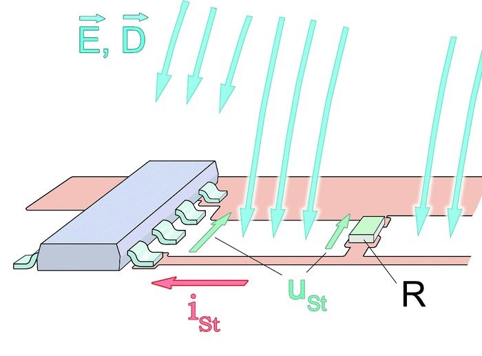
Electric/capacitive coupling
Modules may be exposed to pulsed electric fields of several 10,000 V/m (test set-up according to IEC 61000–4–4) which also affect board networks. A displacement current D flows to the surroundings via the parasitic capacitance of the line. The IC connected to the lines can be affected in two ways:
- The network essentially has circuit elements R, L and diodes against Vdd and Vss on the board and in the IC. The displacement current generates a disturbance pulse uSt at these elements. This disturbance pulse is converted into a spurious signal in the IC by the input circuit and further processed as a logic signal.
- The displacement current is split into two shares. The first share is discharged via the equivalent circuits of the board and any decoupling capacitors that may be present. The second share of the disturbance current iSt flows through the IC via drivers or protective diodes to the Vdd/Vss system. It produces effects similar to those of a magnetic field coupling.
Share:


