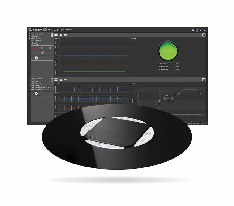
CyberOptics Corporation, a developer and manufacturer of high-precision 3D sensing technology solutions, will launch its WaferSense Auto Vibration and Leveling Sensor (AVLS3) with CyberSpectrum software. Semiconductor fabs and OEMs value the accuracy, precision and versatility of the WaferSense AVLS3 – an efficient and effective wireless measurement device for leveling and vibration.
At only 3.5 mm, AVLS3 can travel with ease to most fab locations where a wafer travels. The Chemically Hardened Glass (CHG) substrate enables smooth wafer handling and improved vacuum chucking.
With long-range wireless capability, AVLS3 combined with new, easy-to-use CyberSpectrum software, collects and displays both leveling and vibration data simultaneously for fast equipment set-up, alignment and real-time equipment diagnostics.
“Engineers in the front-end of the fab can speed equipment qualification, shorten equipment maintenance cycles, lower equipment maintenance expenses and enhance process uniformity,” said Dr. Subodh Kulkarni, President and CEO, “As with other WaferSense devices widely used across fabs world-wide, AVLS3 can significantly improve yields and tool uptime.”
Additionally, for mid-end and advanced packaging inspection and measurement, the company’s proprietary NanoResolution Multi-Reflection Suppression (MRS) sensor technology identifies and rejects multiple reflections caused by shiny components and mirror-like surfaces. Effective suppression of multiple reflections is critical for highly accurate measurements.
Offering an unparalleled combination of high accuracy, high resolution and speed, MRS sensors are widely used for inspection and measurement in the SMT, semiconductor and metrology markets. The new 3– micron NanoResolution MRS sensor enables metrology grade accuracy with superior 100 % 2D and 3D inspection performance for features as small as 25-micron.
Further, it is two to three times faster than alternate solutions in the marketplace. With data processing speeds in excess of 75 million 3D points per second, the NanoResolution MRS sensor delivers throughput greater than 25 wafers (300 mm) per hour. 100 % 2D and 3D inspection can be completed simultaneously at high speed, versus an alternate, slow method that requires two separate scans for 2D and 3D, and only a sampling of a few dies of the 25 wafers.
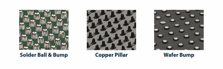
This MRS sensor technology is ideally suited for the inspection of CPU sockets, IC package, solder balls and bumps, copper pillars, and other advanced packaging and mid-end semiconductor applications where high precision and speed are needed.


