Robert Englmaier and Georg Kleemann, two exceptionally experienced laser and software specialists, founded the German stencil and micro-machining company LaserJob in 1992. Right from the very start it was their aim to manufacture laser-cut (SMT surface mount technology) stencils of high quality. Later, they added high-precision micro-machined parts. “First, we realized that there was a large demand for printer stencils, and later also for miniature items which could only be manufactured with high precision using laser equipment”, explains Georg Kleemann. With this mission and the commitment to provide customers with thorough service and support to the minutest details, the company has apparently built up a fine reputation.
So, reportedly, the small, owner-operated company LaserJob from Grafrath has became a pioneer in the innovation and production of laser-cut SMT stencils in Central Europe, and a widely accepted player in this area. At the beginning, the first laser systems were developed by the company directors themselves using high-grade components from leading suppliers. Today, with their profound experience in the laser and software technologies, Robert Englmaier and Georg Kleemann also aid the company staff in providing the maintenance of the laser systems or modify them to meet the individual requirements for their individual in-house applications. This is vital in the design of new areas of application such as the fabrication of the company’s PatchWork or the NanoWork stencils (protected by patents), for example. “Based on our experience and knowledge of laser technology and its different fields of application, we took the chance to develop its use in the other area of tiny parts processing”, Georg Kleemann says.
Laser machining of miniature parts
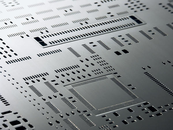
Today the company is operating ten laser systems for the individual applications on its shop floor. About 70 % of its turnover is generated with stencils, the rest with the manufacture of miniature, laser-machined items for a host of different customers and devices. The laser-machined parts can be used, for example, in rework stations, medical equipment, spectacle frames, aerospace, automotive, as well as environmental and measurement instrumentation and more. The material processing expertise at LaserJob encompasses cutting, welding, drilling, labeling and the assembly of the micro-machined part applying laser technologies. The lasers used in micro machining of metals are primarily the solid-state pulse and fiber pulse types, as Georg Kleemann says. Depending on the quality of the beam, focal spots between 10 and 50 µm can be generated, which is adequate for many applications.
Practically all kinds of metals can be processed such as steel, copper, titanium, gold, silver, etc. with thicknesses of up to 1.0 mm, sheet format of up to 800 x 600 mm, and in all quantities needed. For welding, alloys are critical where the melting and vaporization points of the constituents vary greatly, as is the case, for example, with brass (CuZn) and aluminum alloys such as AlMg oder AlSi). The benefits of laser-pulse welding, for example, are the low material warpage, the small heat-affected zone and its contact-free application. The width of structures can be down to 10 µm, minimal cut kerf is 30 µm (standard 50 µm), a processing tolerance of ± 7 µm is guaranteed. In the case of labeling, the energy of the laser provides markings either by removing material from the surface or, via a chemical/thermal process, adding a colored coating. Examples of this are the labeling of anodized aluminum (removal of the anodic coating) and stainless steel (creation of a colored coating). This technology also enables the etching of plastics, or more precisely, the fillers added to the plastics. Many black plastics contain carbon, which is easily bleached creating an almost white lettering. Metals and plastics with a labeling surface of 100 x 100 mm can be processed.
Innovators of SMT stencil technology
LaserJob is reportedly one of the leading suppliers of SMT stencils in Germany and also delivers worldwide. The enterprise has customers in Europe, the US and Asia for all kinds of its stencils, the standard version and especially the PatchWork, wafer bumping and the LTCC (low temperature, co fired ceramic) substrate types. And now the company comes up with its new NanoWork versions. “For the pioneering work we have done here in the stencil design,” Kleemann points out, “with a company of our size we can be a little bit proud of it.” Metal sheets with gauges from 25 to 1000 µm can be cut with an accuracy of ± 5 µm over an area of 800 x 600 mm. The LaserJob stencils are being finalized with a propriety CNC-controlled brushing process, meandering-guiding the brush over the surface in all directions. The brushing does not lead to deformation of the pads, and the material removal is said to be less than 3 µm (surface coarseness approximately 1 µm). As Kleemann points out, the automated, uniform treatment of the whole surface does not depend on staff skills. “It is not a electro-chemical, manually performed etching process, through which the sheet’s thickness is reduced by approximately 20 µm,” he says, “and where the apertures are widened by about 30 µm. Electro-polishing destroys the high precision work of laser technology, therefore we don’t use it”.
A patchwork stencil family
The PatchWork version was originally designed in order to solve the issue with quite different solder paste volumes on PCB pads for very different components. “While other suppliers offer stencils with different thicknesses, we introduced a novel approach due to our patented stencil design”. As Kleemann further explains, “We cut large apertures from the stencil metal sheet in the form of the components, produce a small piece of the appropriate thickness and weld this small item on the normal basis stencil.” With this technology, every special component can therefore be provided with the solder amount needed. In principle, all pad volumes to be put on the stencil surface but differing from the base material thickness capability, say 150 µm, can be lowered (reduced thickness added) or amplified (with an inserted stencil piece of more thickness). This looks like a patchwork then, whereby the resulting stencil sheet thickness is guaranteed within ± 3 µm. Since the weald seam smoothly adjusts the level of the patches, the squeegee can closely accommodate to the outline.
In the semiconductor, backend Si-wafers are being supplied with numerous small solder balls as connecting terminals of the respective ICs (when singulated later) by means of printing small amounts of solder paste through huge stencils, featuring hundreds of thousands of tiny apertures on a very large area with very high precision. Up to 250,000 single solder volumes are to be printed in one stroke. The density can be up to 16 pads per sqmm. To manufacture these stencils, LaserJob has designed techniques which guarantee correct scaling even with a high pad density, since the solder amount directly influences the bump height. Tolerances within an IC are limited to just a few microns. Through the addition of an optional reinforcement ring, detaching the wafer from the stencil more evenly avoiding a trampoline effect possible, even better control can be achieved. With a stencil thickness and aperture outline tolerance of within ± 3 µm, the precision needed can be achieved, where the surface coarseness is Rz < 0,9 µm. Especially together with the newly introduced nano coating technology, this stencil type offers the next step of precision in wafer bumping, as application manager Carmina Läntzsch explains. In an elaborate process, the laser cut SMT metal stencil can be coated with nano-size particles. „This considerably increases the wetting angle of the surface,“ says Georg Kleemann, „and the adhesion forces between paste and stencil decreases.“ The solder paste cannot adhere to the apertures and slides off the surface at the cut edges.
Let’s have a look at the benefits
Working with a certain stencil thickness, smaller patterns than usual can be cut due to improved release properties. The compromise between stencil thickness and the amount of soldering paste required for fine-pitch components is smaller, so the user need not focus on the release properties when choosing the thickness. He may instead take into account the actual amount of paste needed. The NanoWork stencil offers extended capabilities for PCB layout, especially with regard to the ongoing component miniaturization and fine-pitch design, enabling the application of advanced packages. The user needs far fewer cleaning cycles due to the non-sticking properties of the coating. This leads to an increase in printer capacity of at least 10 %. As he constantly uses the same amount of paste, the dependability of the soldering process is highly improved. In addition, there is far less need for board rework.
Finally, the company is a proven supplier of LTCC stencils for hybrid manufacture. “We were the first in this field of application,” says Kleemann. The different layers of the ceramic substrate are connected by vias which have to be filled with tin-silver paste. The stencil positioning in regard to the substrate, together with the maximum process tolerances, require that the respective acceptable tolerances are minimized as far as possible for every process step involved. “We have a very tight quality control and assurance strategy for the stencils manufactured,” he finally explains. “To begin with, we are certified according to DIN ISO 9001:2000 quality assurance system.” The production is then being controlled by cross-section samples and applying an OKM measuring system. “For the end control we use measuring microscopes (accuracy ± 1 µm), as well as stereo microscopes and image analysis for the verification of the metrics,” Georg Kleemann concludes. (gbw)
SMT, booth 9-225
EPP Europe 415
Share:


