National Physical Laboratory, NPL, interactive assembly and soldering defect database is available to all EPP readers. This allows engineers to search and view countless defects and solutions or submit their defects on line at http://defectsdatabase.npl.co.uk/
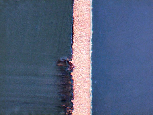
The microsection image ( figure 1 and 2) shows PCB through hole copper plating pulling away from the surface of the laminate. Copper separation from the surface of the hole is not very common in industry, or not for so many years. It has been seen in recent years with lead-free.
Recent use of higher Tg laminates which require modification in the plating process to successfully key the copper to the hole wall have been experienced. Any poor or lack of adhesion would increase with the high soldering temperatures and moisture content during lead-free assembly. It is necessary to work with the PCB supplier and examine the testing conducted for different laminate materials. Thermal shock testing on samples and microsectioning is the simplest test method to consider to prove any improvement in the copper plating adhesion. Thermal shock testing is best conducted with a sand bath rather than a solder bath and the lack of copper adhesion is easier to identify. Solder filling the plated through hole during test tends to support the copper.
The database is a resource for readers to search or submit problems online with possible solutions at http://defectsdatabase.npl.co.uk/
EPP Europe 414
Share:


