Amicra Microtechnologies GmbH, a worldwide leading provider of high-precision micro-assembly equipment and customized electronics manufacturing solutions, comes to this year’s Semicon West to demonstrate its latest advanced die and flip-chip bonders AFC Plus and NOVA Plus. Both systems are perfectly suited for die and flip-chip processing including 3D and stack-die, covering the full scope of high-volume micro/nano assembly applications. They are laid out for bonding processes, offering optional flip-chip bonding, wafer mapping, and post-bond inspection.
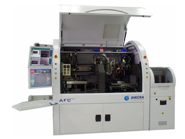
The ultra-high-precision Amicra AFC Plus bonding system was designed as a modular concept for utmost user flexibility and customer accommodation. AFC Plus realizes a placement accuracy of +0.5µm at 3 Sigma for die and flip-chip attach. At a cycle time of <30sec, it is well suited for processing micro-optic and micro-mechanic components, with eutectic bonding via diode laser or heating plate. The system provides auto loading of wafers and substrates, wafer mapping, epoxy stamping and dispensing. Active alignment is provided on request. Post-bond inspection is included; UV curing is featured as an option.
The new NOVA Plus die-attach and flip-chip placement system, introduced in 2010, offers a combination of high accuracy (+2.5μm at 3 Sigma) and high-speed processing at a very low cycle time of <3sec. Auto-loading is provided for wafers up to 12inch (300mm) diameter and up to 450mm substrate wafers, with a substrate working area of 500x500mm. With these specs, the system is well suited for today’s preferred bond processes such as eutectic, epoxy, and laser bonding. Alignment is passive, with active bond force control. The modular concept is well suited for micro-assembly applications, multi-flip-chip bonding, wafer mapping, and post-bond inspection I various industrial segments. Post-bond inspection and measurement are provided as a standard feature, UV curing and dispensing as options. With its broad product line of semi-automatic (SIS) and fully automatic wafer ink (AIS) systems, the company is currently setting industry standards at a dot size down to 125µm, and for the inking of diced or undiced wafers. The AIS system enables inking of 12-inch wafers, at a dot size down to 70µm. The LTS test system is a flexible multi-bin test and sorting system for Laser Diode and LED components, accommodating up to three test stations. First delivery of the system was in 2012, since then, multiple systems have been installed at a major European LED manufacturer. In addition to its line of standard products, the company offers customized processing solutions for gel dispensing, LED inspection and test, as well as in-line integration of these systems.
Share:


