


In recent years, Package on Package (POP) and Bottom Termination Components (BTCs) devices have become very important and widely used in the PCBA manufacturing process. Two of the most challenging PCBA process failures are component warpage and HoP defects. Therefore, achieving the best possible solder joint quality becomes an increasingly important consideration for the PCB assemblers. Most of the solder joints of a POP and BTC device are invisible by optical means, so X-ray inspection is the only way to examine the solder quality in a non-destructive way. At the same time, the only method for assessing the warpage and co-planarity issues of the component is 3D AOI.
As a consequence, AXI and 3D AOI are more frequently used on the SMT lines. However, both these technologies have certain limitations that may need assistive technologies for the verification of possible false faults. The false-fault rate of the inspection system, one of the key items of the fault coverage, affects the overall efficiency of defect detection. Simply put, the more false faults you pass on to a repair station for validation, the more real defects could get missed. False faults generate costs. Each defect reported by AOI or AXI must be verified. If the reported defect turns out to be a false alarm, then its verification effort is a cost that could have been saved, because the verification did not create any real value. False-alarm verification costs include labor, capital equipment and other related costs such as factory overheads and panel handling.
Due to the continuous miniaturization of SMT components and increasing complexity of the assemblies, false faults have not been eliminated so far and smart verification strategies should be implemented.
Component warpage and Head on Pillow (HoP)
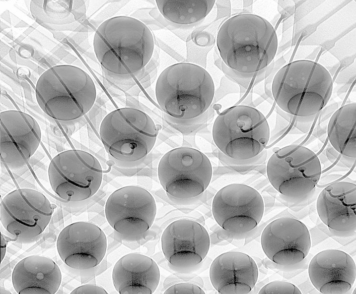
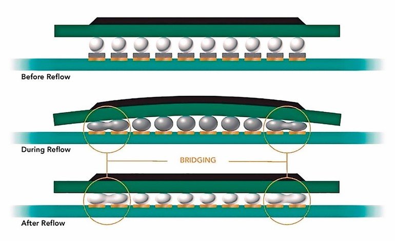
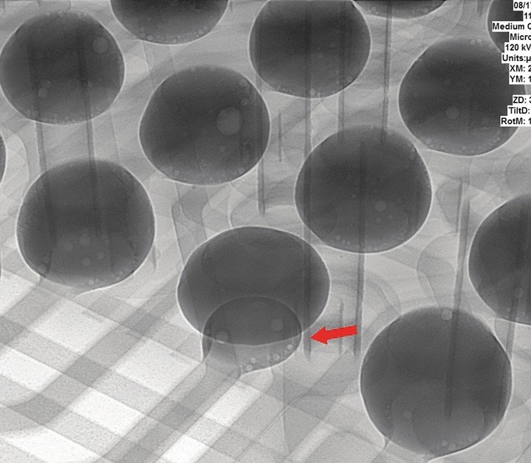
Component warpage: For PoP packages, the warpage issue is always one of the most difficult for SMT process engineers, because it is easy to cause an open solder joint problem. The typical SMT defect modes, such as non-wet open, solder bridging, head and pillow, and non-contact open are applicable to both the joints between the PoP bottom package with the board and the PoP memory package.
Package warpage is widely recognized as a primary factor in the formation of HoP. In fact, several industry consortia efforts are currently in progress to help characterize factors influencing package warpage behavior in an attempt to define mitigation measures. These include the iNEMI Package Warpage Qualification Criteria and the HDPUG FCBGA Package Warpage projects.
Virtually all BGAs warp, certainly plastic ones and some ceramic, and particularly those that have a complex internal structure and are not thermally balanced. In the case of a BGA warping, the corners have the largest displacement causing open and, potentially, bridges due to warping up (concave) and lifting above the circuit board or warping down (convex) and pushing into the solder paste, therefore causing bridges.
Once a solder is open, the board will fail in the function or reliability tests and will need to be reworked. In addition, the rework of PoP packages is a challenge compared to the normal, single BGA. It is therefore critical to avoid unnecessary rework, if the connection is still reliable despite the warpage of the component.
HoP: Open circuit at the ball interface is an increasingly problematic failure mechanism, since BGA components have been converted to lead-free alloys, lead-free solder is the norm in assembly and higher reflow temperatures are needed.
However, there is some confusion about this critical defect. Head-on-pillow defects can often be attributed to a chain reaction of events that begins as the assembly reaches reflow temperatures.
Components generally make contact with solder paste during initial placement, and they start to flex or warp during heating, which may cause some solder spheres to lift. This unprotected solder sphere forms a new oxide layer. As further heating takes place, the package may flatten out, again making contact with the initial solder paste deposit. When the solder reaches the liquidus phase, there is insufficient fluxing activity left to break down this new oxide layer, resulting in possible HoP defects. Warping of the PCB causes the same fault, as does insufficient solder paste and poor stencil aperture design.
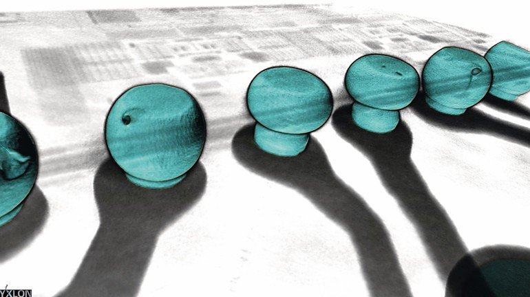
On the other hand, HiP defects are actually very rare and even harder to detect. In this case, the shape of the solder ball may not have changed. The solder paste has reflowed, wetting the pad and molding around the solder sphere. This type of defect is also referred to as ‘ball-in-up’ and many other names. A HiP defect can appear if the preheat time is too long and/or the dwell temperature is lower than required and the flux exhausts its activation and cleaning capability. In both cases, due to the lack of solder joint strength or contamination, these components may fail with very little mechanical or thermal stress. Eventual separation of what was never a proper metallurgical bond can lead to late-stage manufacturing defects and even early-stage field return issues.
This potentially costly defect is not usually detected in functional testing but can be detected by X-ray systems. If not detected, these only show up as failures in the field after the assembly has been exposed to some physical or thermal stress.
3D AOI as a sensor
The continuing evolution toward advanced miniature packaging has led to ever increasing PCB density and complexity. As the manufacturing process becomes progressively more complicated, there is an ever increasing probability for defects to occur on finished PCB assemblies.
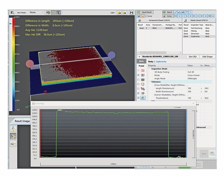
For years, the Automated Optical Inspection (AOI) industry has relied solely upon two-dimensional (2D) inspection principles to test the quality of workmanship on electronic assemblies. While advancements in conventional 2D optical inspection have made this technology suitable for detecting such defects as missing components, wrong components, incorrect component orientation, insufficient solder, and solder bridges, there is an inherent limitation in the ability to inspect for co-planarity of ultra-miniature chips, leaded devices, BGA and LED packages. True co-planarity inspection of these challenging devices is an absolute necessity and requires the addition of a third dimension in inspection capability: 3D inspection technology.
Although 3D inspection technology has existed for many years in the electronic inspection industry, this technology has primarily been reserved for inspecting solder paste depositions on printed circuit boards directly after the screen printing process. Over the past few years, however, 3D inspection has emerged as a viable technology for testing gull-wing and BGA devices as well as a host of other co-planarity sensitive circuitry on finished PCB assemblies. Of course, the main reason for the industry trend toward 3D inspection technology is to compensate for the limitations of conventional 2D inspection.
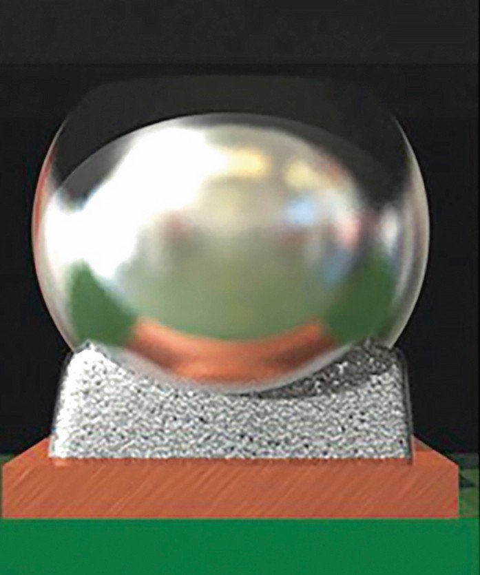
The only limitation of 3D AOI is that it is an optical inspection system – it cannot see underneath any black devices, such as BGA, PoP, QFN, etc. Therefore, it does not allow the system to make a conclusive decision if the solder joints of the black devices are still acceptable, despite co-planarity or warpage issue.
If one side of the BGA is lifted, it requires an additional verification in an off-line X-ray system or under a microscope. Manual inspection is always slower and more costly, but in many cases, it is the only way to verify the findings of the in line systems. In this particular case, the reason for co-planarity was one loose, small component underneath the BGA.
AXI as a sensor
The use of AXI for printed circuit board inspection continues to grow in manufacturing, especially on high-density/high complexity boards. The AXI is an effective test tool for solder joint inspection, and it usually detects about 90 % of the total defects on a circuit board assembly. The AXI uses 3D X-ray testing to locate manufacturing defects; this is especially important to increase coverage on boards with limited access. The AXI pinpoints the exact location of defects, and thus repairs are both fast and inexpensive. The AXI is an ideal tool for testing high-reliability boards with medium-to-high-complexity designs and components that have limited visual and electrical access. The AXI covers most of the process fault spectrum, including short, open, insufficient/excess solder, misaligned and missing components, reversed polarized capacitors, and even unreliable solder joints that might escape electrical tests.
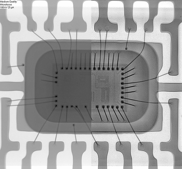
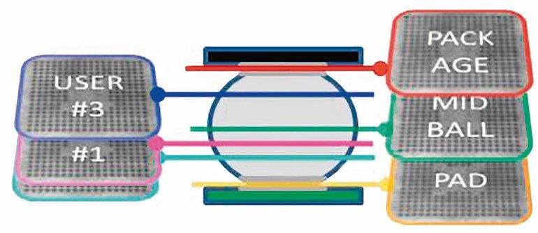
One of the challenges in AXI performance is to detect HoP and open defects for optically hidden solder joints, such as BGA, BTC, POP, and other advanced packages. The in-line X-ray inspection systems try to find HoP defects by looking at BGA balls in at least 3 different positions – the PCB Pad slice, the BGA Mid-ball slice and The Package Slice. The images are automatically analyzed with the original CAD-based designs and user definable settings.
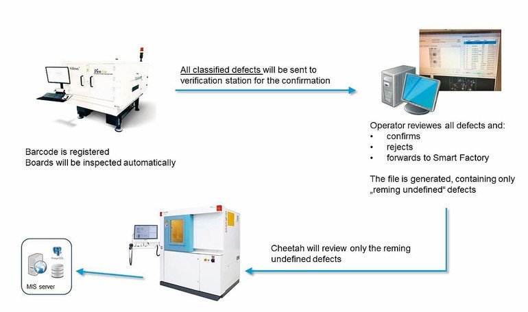
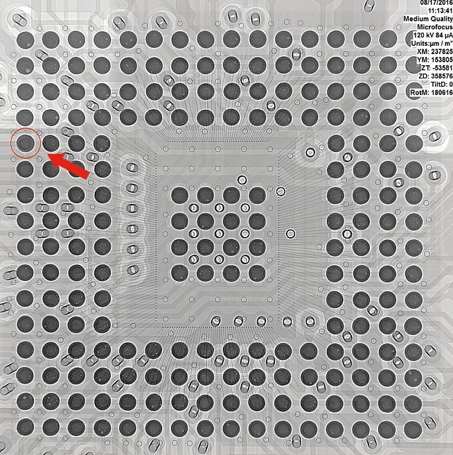
The advanced algorithms and adjustable magnification allow defining if the particular ball is smaller or bigger than its neighbors. With challenging components, the number of slices can even be increased, but then the required time also increases. However, most in-line X-ray inspection systems have rather high false-fail rates. False failure calls cannot be eliminated completely, but the rate must be reasonable for the production line. These findings should be confirmed either on a verification station or inspected again on a high-end at-line X-ray system.
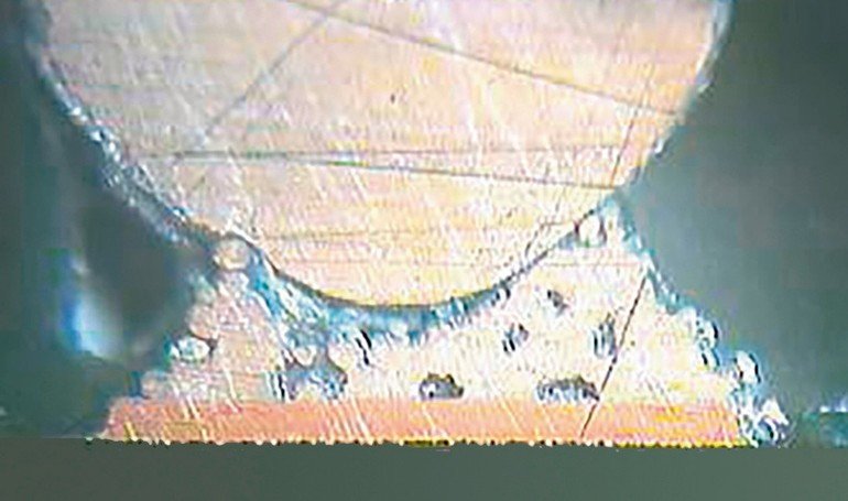
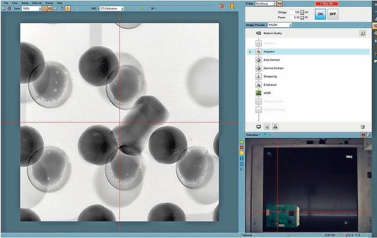
The reason is simple: AXI can easily detect HoP joints at standard magnification, but if the BGA ball size falls below 250 microns, this becomes much harder even at high magnification and it is more likely to miss HoP defects. In these situations, the proper search of HoP defects requires high-resolution oblique view images. These high-resolution images can be generated by an off-line or at-line X-ray system. These systems have mostly open-type transmission X-ray sources, and some can perform in three different modes – nanofocus, microfocus and high-power modes. Due to the mechanical design, an at-line system can also gain better 3000 x geometrical magnification.
Most importantly, more advanced development of the image chain in at-line systems allows processing images during the image stream. As a result, all the images viewed on the monitor are enhanced. The distinction can be significant. When viewing a crack in a solder ball, for instance, instead of selecting images that appear to best show the crack and then processing those images, the viewing of an enhanced image of the crack can occur in real-time, while the position of the sensor (or the specimen) is changed to provide multiple viewing angles. Another high-value tool for live image analysis is μHDR which involves averaging the exposure of the overall image and showing in glance the structure of the sample object.
Smart factory
As said earlier, smart manufacturing should be a proactive and independent decision-making environment where connected systems or machines will “talk” to each other. That “discussion” is, however, based on algorithms. By definition, an algorithm can give us only one single answer. But does this provide us with the right answer or one out of three or four or five alternatives? Will it provide the same response every time or different ones for the same issue? Many MIS systems are not ready to manage big data due to the lack of smart analytic tools. Without human intervention to make those critical decisions, based on knowledge and experience, we still cannot talk about completely effective and efficient smart production. Therefore, the reliable solution combines human brains and algorithms, allowing Process Managers to make informed decisions after seeing all the data from various collection points. This data is relayed to a single screen that also provides historical information and everything needed to make a truly informed decision. This is definitely a ‘smart solution’; it is not a ‘lights-out’, fully automated Smart Factory, but it is much better than many factories today. It allows the real-time monitoring of production flow and the changing of settings and limits to ensure that the product produced remains within the optimum process window, yielding a potentially 100 % acceptable product coming off the line, at least in terms of assembly defects. It is also a big step towards “full automation” and, therefore, well worth embracing as a way of improving yields and reducing costs.
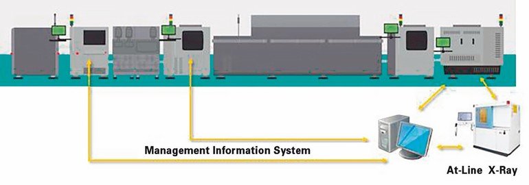
Considering all this, an at-line X-ray system should become an additional high-end sensor that can compensate, for example, for the limitations of AXI or 3D AOI.
An at-line system is essentially an off-line system that is linked to the production line and placed beside it, allowing real-time response to issues and making the X-ray system a tool of the production and QA teams and not simply a test machine in a lab, used by QC staff.
This solution is simple to implement and, therefore, reliable. The at-line X-ray can be connected to an in-line 3D AOI or in-line AXI inspection system directly where it becomes a smart verification tool, where only questionable and unsolved faults will be transferred for repeat inspection on a high-resolution at-line X-ray system. The inspection results can be stored on the system PC, but can also be exported to the customer’s MIS.
The connectivity of the at-line system is based on Internet Protocol (IP) via Transmission Control Protocol (TCP). Further use of data (collation and visualization of results from different inspection systems) will depend on the end customer’s demands and capabilities. The collected data allows us to understand what has happened in the past to make predictive analyses about future trends. The general task is to provide a dashboard view to the Process Manager who can track down the possible problem areas and initiate proactive measures to improve the quality of production, before rejects or scrap units are produced.
Added value of smart factory
The ultimate target for this solution is to increase production yield and reduce the manufacturing costs, including troubleshooting and rework. In high-reliability products, for instance aerospace, military and automotive, there is no room for uncertainties. All possible defects have to be verified and reworked. Conventional methods for troubleshooting are the ICT, microscope, etc. These are usually quite expensive and should be avoided at any costs.
As a reference, we can use 700 USD as the hourly cost of the ICT method (incl. technology, labor and overheads). 400 USD per hour will be an average cost of a PCB rework. Obviously, these numbers vary from country to country but should reflect the industry standard. The value of this smart factory to the user will be on-demand locations scanned from 2 different inspection systems – 3D AOI and X-ray – which can be compared side-by-side so that the user can make an informed and conclusive decision on the defect calls.
Conclusion
Based on our studies, we conclude that the AXI and 3D AOI algorithm threshold settings are critical for detecting certain PCBA process failures. The AXI and 3D AOI program optimization is based on its measurement data analysis. Per current AXI and 3D AOI performance, it is beneficial to utilize the AXI or 3D AOI equipment jointly with an at-line X-ray system for verifying defective location for AXI and 3D AOI algorithms optimization process. A solution like smart factory can add value in different phases of production. The major value of smart factory comes from regular production, where a company with an average production yield of 90 % can increase it to 99,5 %. At the moment, the best smart factory quality control solution is the combination of human brainpower and algorithms.
References
SMTA: BTC: Bottom Termination Component or Biggest Technical Challenge? Greg Caswell and Cheryl Tulkoff, ASQ CRE
SMTA: Optimizing x-ray inspection with package on package: David A. Geiger, Zhen (Jane) Feng, Ph. D., Weifeng Liu, Ph.D., Hung Le, Tho Vu, Anwar Mohammed, Murad Kurwa
SMTA: Collaboration between OEM and EMS to combat head on pillowing defects, Alex Chan, Paul Brown, Lars Bruno, Anne-Kathrine Knoph, Thilo Sack, David Geiger, David Mendez, Mulugeta Abtew, Iulia Muntele, And Michael Meilunas
SMTA: Automated x-ray inspection: SMT process improvement tool, Zhen (Jane) Feng, Jacob Djaja, and Ronald Rocha
Package-on-Package Warpage Characteristics and Requirements; Wei Keat Loh, Intel Malaysia, and Haley Fu, iNEMI
Head-in-Pillow BGA Defects; Karl Seelig, AIM
Acknowledgements
- Keith Bryant, Technology Consultant
- Bob Willis, Bobwillis.co.uk
Zusammenfassung
Der Artikel zeigt, dass derzeit die beste intelligente Lösung für eine Qualitätskontrolle in der Elektronikproduktion die Kombination aus menschlicher Intelligenz und Algorithmen darstellt.
Résumé
L‘article indique qu‘à l‘heure actuelle, la solution la plus adapté pour le contrôle de qualité dans la production électronique est une combinaison d‘intelligence humaine et d‘algorithmes.
Резюме
В статье рассказывается о лучшем на текущий момент интеллектуальном решении для проведения контроля качества электронных продуктов, представляющем собой комбинацию человеческого интеллекта и алгоритмов.


