Printed electronics using conductive paste represents a trend reversal in electronics manufacture: new product features, new functions and simplified production processes will in future drive the technology. However, the printed layers are too thin to achieve the required electrical properties. With multilayer printing, several layers can be printed on each other in order to obtain reliable structures on electronic substrates.
Michael Heilmann, Franz Padinger, Franz Plachy, Asys subsidiaries Ekra and Botest
The Asys company Ekra offers special thick-film solutions in the Hycon product portfolio. Besides standard SMT applications, Ekra has specialized for decades in products for special niche markets such as printing on ceramics, glass, wafers, flexible foils, but also on direct printing of functional layers on these materials. The subsidiary Botest is also member of the Asys group, specializing in paste development as well as developing and optimizing printing processes. The research lab in Linz/Austria designs advanced elements of printing processes such as screen, stencil and printing medium, and provide them for application-specific requirements. Dedicated solutions optimally matched to customer-specific procedures can thus be offered from a single source.
The printing of electrically conductive pastes can open novel manufacturing methods for the electronics industry. However, the conductivity of the ultra-thin layers, which are often only a few microns thick, is extremely limited. Larger currents can be conducted over tiny printed traces only with significant electrical losses or simply lead to dangerous overload. Combined with high printing resolution, this kind of manufacture is challenging machine and material. Machine designers, process specialists and paste developers are requested here to create the technical conditions for precise multilayer printing.
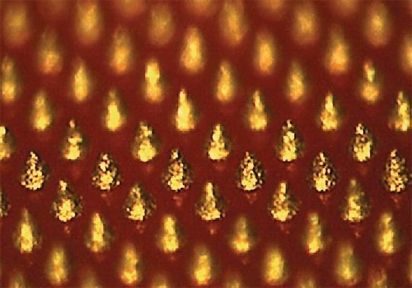
The figure shows prints made with electrically conductive paste and an excellent ratio between print dot height and print dot diameter (aspect ratio). The dots have a diameter of approximately 70µm and require for their function as elastic contact pads a height of also 70µm. The distance to neighboring contact pads is also about 70µm; the dots have a staggered structure. With an active print area of 180mm x 255mm, this results in approximately 2.3 million contact pads on this substrate. Stencil printing was chosen as the preferred method of use, with up to four layers sequentially printed one above the other, to achieve the desired aspect ratio of nearly 1 and to be on the safe side with current loads.
Printing parameters
An Ekra in-line printing system was used for placing the dots on a flexible PE film substrate. The aluminum print nest featured glued poroplastic material and vacuum suction. This allowed for creating a highly homogeneous support surface for the substrate.
The printing paste was specifically developed by Botest to achieve the parameters needed in regard to conductivity and elasticity of the pads to be produced. Thus, the rheological properties of the paste could be perfectly adapted to the printing parameters and the coating of the stencil.
The stencil was pre-flooded while printing the electrically conductive paste. Although this is uncommon in stencil printing, it is indispensable here in this particular process.
After the printing, the processed substrate was removed and dried in an oven. To prevent the foil from warping due to influence from temperatures or from humidity, it was again then assimilated to the environmental parameters after drying. Before the next printing step, the substrate had to be precisely positioned on the printing table. This was provided by using the patented optical positioning system EVA featured in the Ekra printer. In addition, the gap between the substrate and stencil and the down-stop at the squeegee head had to be accurately adjusted to prevent the paste from flowing under the stencil. For the entire manufacturing process this step was repeated up to four times, so that the required height of the contact pads could be reached.
Influences of the process parameters
The printing results could be optimized by tuning three following variables: stencil design, process parameters and paste. In the following paragraphs we evaluate the impact of the most crucial parameters on the printing process.
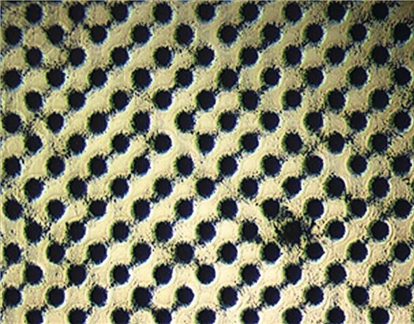
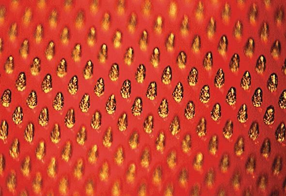
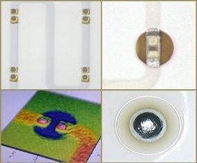
Squeegee angle: The figure shows microscopic images of prints with squeegee angles that are too steep or too flat. So, if the squeegee angle is too steep, the printing paste smears below the stencil, creating a smudgy image. This in turn would cause shorts between the individual contact points. A squeegee angle that is too steep leads to uneven filling of the stencil openings.
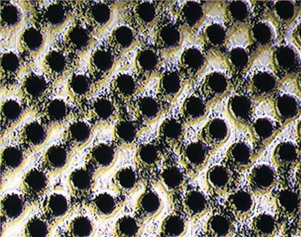
Squeegee pressure: Excessive squeegee pressure, just like a flat squeegee angle, results in smearing of the paste below the stencil and hence leads in a smudgy, distorted print image. This deformation of the pads also makes the exact positioning of the next printing layer difficult in multilayer printing. In addition, the print dots are spreading due to the excessive squeegee pressure, which also increases the risk of shorts. Continuous monitoring of the squeegee pressure and closed-loop control of the printing allow a homogeneous distribution of the pressure over the entire squeegee path.
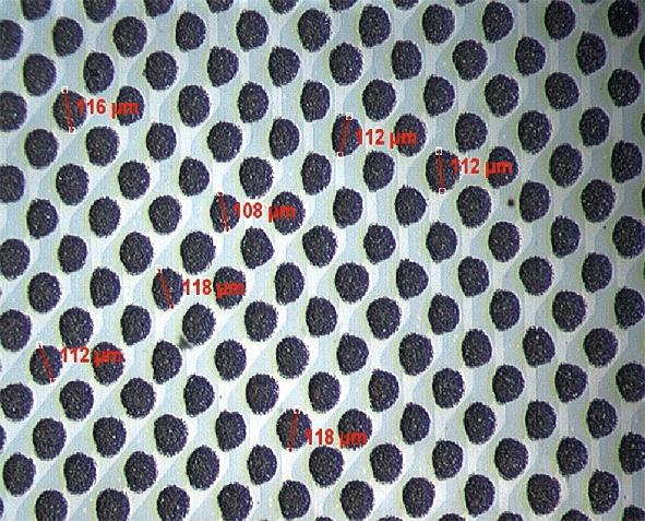
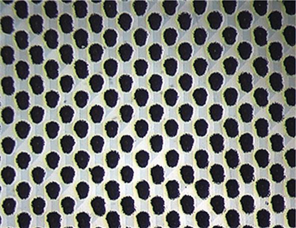
Print direction: An essential factor in high-resolution multilayer printing is the print direction as the squeegee pressure slightly “warps” the stencil. If the print direction changes while the multilayer print is being processed this negatively affect the printing result. The underlying dots can no longer be matched despite precise positioning by means of the EVA alignment system. In this case, there can be deviations of more than 20–30µm per layer, as shown in figure. This offset can be determined and compensated by entering correcting values in the machine software.
Positioning accuracy: To obtain the best possible positioning accuracy, it is important to align the layer to be printed only with the base fiducials. If other markers are used for the alignment, for example fiducials that were printed later, the deviations accumulate. In a finished multilayer print consisting of four layers, the difference with regard to repeatability could be optimized and an overall deviation could be reached for 4 layers of ±12.5µm. This result could be achieved using the optical positioning system EVA and using only the base fiducials for alignment.
Results
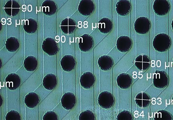
By evaluating the optimal parameters, it was possible to achieve very good print results (figure). Thanks to multilayer printing, the base of the contact pads reaches from 65µm to 70µm (monolayer printing) to approximately 85µm to 93µm, as shown in figure. The adjacent pads not contacted on the underlying base electrodes structured in the ratio of 70/30 (70µm wide and 30µm distance to the next dot). This allows proper electrical functions of the elastic contact pads. The figure shows the height of the individual contact pads. Thanks to multilayer printing, a height of 55µm to 65µm could be achieved for the individual contact pads, which corresponds to an aspect ratio of approximately 0.8.
Conclusion
Because of the optimum interaction between printing parameters and paste, the results for high-resolution multilayer printing could be remarkably improved. With an optimized aspect ratio in multilayer printing, it is possible to create highly conductive structures. They can be used for efficient conduction of currents and represent an attractive option in electronics manufacture. A prerequisite for the best possible positioning of the solder deposits is a high-precision stencil and a very precisely operating printer. With the use of advanced machine features such as closed-loop squeegee pressure control, highly accurate optical positioning system and a variety of different alignment options, the Ekra printer delivers the precision and process stability required. Besides, the drive unit with its servo motor and resolver provides an additional built-in scale with a high resolution of 1µm. This allows precise monitoring and, if possible, correcting the target position even in case of mechanical wear.
All Ekra stencil printers are equipped with these features so all applications can benefit from the mentioned advantages. The exact placement of minimized solder paste deposits, as required e.g. for the component size 03015, is available in the in-line systems Serio and the new 4000 printer platform as of today.
SMT Hybrid Packaging
Booth 7-550
Zusammenfassung
Mit dem Druck von leitfähigen Pasten auf Substraten ist die Elektronikindustrie in der Lage, noch kompaktere und leistungsfähigere Schaltungen und Geräte herzustellen. Nachdem jedoch einzelne Lagen jeweils nur wenige Mikrons dick sind und damit die Stromtragefähigkeit äußerst begrenzt, muss man sequentiell mehrere Lagen mit höchster Präzision übereinander drucken. Dies stellt große Herausforderungen an die Druckgenauigkeit des Printers sowie an Schablone, Rakel und die Paste. Wichtig ist hier, dass von Prozessspezialisten eine Lösung aus einer Hand offeriert wird, damit Anwendern eine funktionsfähige, schlüsselfertige Lösung zur Verfügung steht.
Avec l’application de pâtes conductrices sur des substrats, l’industrie de l’électronique est désormais en mesure de réaliser des montages et des appareils encore plus compacts et plus performants. Compte tenu de ce que certaines couches ne font toutefois que quelques microns d’épaisseur et qu’alors la capacité conductrice est extrêmement limitée, il faut de manière séquentielle appliquer plusieurs couches superposées avec la plus grande précision. Cela représente de grands défis quant à la précision de l’application du printer, mais aussi du gabarit, de la raclette et de la pâte. Ce qui est important ici, c’est que des spécialistes des processus apportent une solution à partir d’une source unique afin que les utilisateurs disposent d’une solution capable de fonctionner correctement et livrée clé en main.
Share:


