
It is well accepted that a high proportion of the defects generated in an SMD line can be attributed to the print process. If these defects can detected immediately after the printer, then the defective PCBs can be removed, cleaned and reprinted, or repaired at this stage. This ensures that only acceptably printed boards are populated, reducing subsequent repair costs and contributing to increased yield from the line. The cost of rework increases as the PCBs progress through the line so the earlier they can be detected then the lower the wasted cost. There has also been a major driver from automotive customers manufacturing safety products, such as air bag sensors and braking systems. The cost of failure in such products during use is very high. Producers are not allowed to clean PCBs with defective prints. Boards with unacceptable printing have to be removed from the line and scrapped. It is understandable therefore that there has been a considerable demand to monitor, and indeed control the print process. Initially 2D SPI solutions were considered adequate; however experience has demonstrated that 3D SPI gives more information and thus better control of the process. There are now many suppliers offering 3D SPI to facilitate both inspection and control. This article offers some points for consideration when choosing a suitable 3D SPI solution.
Chris Davies, Vi Technology, Grenoble (France)
As the PCB progresses through the line the product added value and also the cost of rework increases. There is a considerable benefit to be gained such as reduction in rework costs, by identifying and dealing with the defects as early as possible in the SMT process. Of course the major benefit is gaining control of the solder paste process to ensure higher quality joints and this higher yield at the end of the line. The most basic solder errors that must be identified would include volume, height, surface area (2D shape) bridges, 3D shape, and co planarity. In addition it would be useful to find any contamination of the paste or pad.
3D SPI inspection techniques
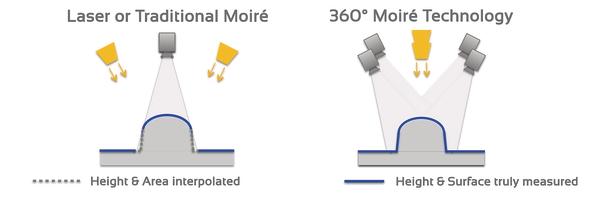
Many inspection companies now offer 3D SPI solutions which meet many but not all of the customer requirements. The majority of systems offered use one of two major techniques, either laser scanning or some form of Moire fringe technique to develop a 3D image.
In most systems, the solder paste deposit is viewed with a vertical camera, yielding X and Y measurement of the surface. At the same time, either a laser raster or moiré fringe is projected onto the surface facilitating height measurement by monitoring the pattern shift, at various positions. A volume measurement is derived by multiplying the X and Y measurement by the height measurement. Is this true 3D?
A number of issues arise, with conventional solutions, which cause some concern with these techniques.
- The first issue relates to the reference used for measuring the paste height. Systems often search for a local reference near ideally on the pad, some using more than one such reference point. These can be subject to error caused by small displacement, if for example the reference point used is not actually on the pad.
- The second relates to the position and angularity corrections that must be implemented to cope with PCB warpage. This at best is time consuming, often involving mechanical movement and can cause further inaccuracies in reference measurement.
- The third relates to the frequency of fringe (or laser raster) used to generate the 3D image. The frequency determines both the range and resolution of the measurement. In order to resolve typical paste heights (In the region 100 – 120 microns) some systems only measure above a fixed height perhaps 40 micron. They assume that the area under this threshold is solid.
- The forth concern relates to the position of the orthogonal camera, which offers a 2D view from above only, necessitating some kind of imaginary construction of the side of the deposit.
A newly introduced and innovative technique known as 360° Moire generates a true 3D image and provides the capability to better address these requirements by eliminating many of the these issues of concern evident with existing systems.
Revolutionary new solution
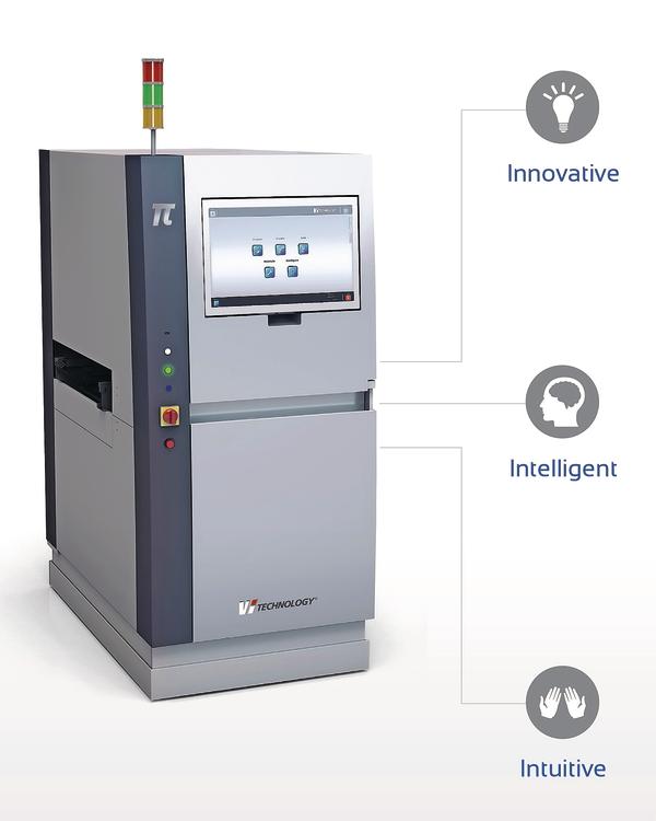
360° Moire is the technique used in an innovative true 3D SPI inspection machine developed by Vi Technology and called Pi. Pi is Innovative, Intelligent and Intuitive and allows the customer to see and measure the print process like never before. This new technology, covered by 10 patents, utilises the latest techniques in image acquisition, lighting and algorithms to provide a true, easy to use production tool. With 100 times more computing power than conventional solutions, the solution provides an ultra large image in 3D true colour. It provides a large PCB capability (up to 533 x 600mms) within a very small envelope (only 800mms wide) responding to the increasing constraints on floor space in modern SMD lines. A number of models are offered, to suit customer needs and budgets, each model delivers the same quality of inspection, the only choice is to select a model with inspection speed to match the SMD line. Windows operating system was not fast enough to match the speed that the processing of full real time image manipulation demands. For this reason, Linux was chosen as the operating system because it is much less susceptible to virus infections.
A natural user interface (NUI) has been designed from the outset to offer convenient and intuitive operator interaction. Pi does not have either a keyboard or a mouse. All instructions and controls are easily carried out using the touch sensitive screen. Indeed many users immediately feel comfortable operating the machine with as little as 10 minutes training! The solution does most of the work automatically for the operator. The initial steps of converting the Gerber data into a pad file and entering the basic customer data can be accomplished with web based tool called Sigmalink included with each machine. This minimises the activity required on the machine itself during product changeover, maximising production throughput. Previously programmed products are presented in a rotatable carousel with full PCB image view to quickly and easily identify and reload a product inspection program for further production.
Pi automatically configures tolerance settings, which can be replicated again when similar products are processed in the line. It is usual to set different tolerances for different pad geometry. Clearly the tolerance on a 0201 resistor pad (relatively small volume of paste) would not be the same as for example a large area thermal pad. The use of area/roof ratio, commonly used for stencil design, is utilised to set the optimum tolerance for each different pad geometry. In most cases, tolerances are set for groups of similar shape pads.
The process engineer has the capability to select expert mode where full flexibility is provided to modify and set discreet tolerances. The tolerance thus set can be named and saved, and offered in a look up table for the operator for future programming of similar product. Embedded SPC capability allows for the monitoring in real time of process trends, providing the warning or stimulus perhaps to initiate stencil cleaning. Pi also includes an embedded on board calibration jig, allowing periodic calibration of both mechanical and optical values ensuring consistent and repeatable performance as well as cross platform program transferability. Straight forward interface modules can be configured to provide feedback to Stencil printers. Currently most customer chose only to modify stencil position offset, (X and Y).
There is much work under way to determine the criteria to initiate stencil cleaning (either wet or dry). This offers potential savings in cost (solvent and paper), as well as significant throughput benefits. Current practice for many customers would be to select a cleaning frequency that from experience ensures minimum number of problems. In some cases, for a complex product, this may be after as few as two PCB. In such a case if the print time is say 10secs and the clean time is 30secs, then the time for 2 PCB would be 50secs. (2 x 10 + 30). This means a line rate of 25secs/PCB. If the cleaning frequency could be extended to 4 PCB then the rate becomes 17.5secs/PCB, a throughput increase of 30%.
How to select the optimum SPI solution
When choosing the best solution for your SPI inspection, a number of key attributes must be considered including:
- The length of time required to train the operator to use the machine. This can be particularly important where there is a high turnover of staff
- The ease of programming, as this will determine the skill set required to operate the machine, can this be done by an operator or does it require a process engineer
- The speed of programming, how long does it really take to get into production
- The cycle time (can the SPI match my line rates)
- Inspection validation, gaining confidence in the equipment and trusting the results
- And not least the reliability, accuracy and repeatability of the results.
Generally programming of an SPI machine is regarded as easy (Compared to an AOI) and considered to be quite fast. However there are more steps to be considered than might at first be evident.
- Gerber to pad conversion. This is usually carried out with a 3rd party software such as EPM for example. Some 3D SPI systems now offer in house data conversion. A typical example would be Sigma link which can provide front end data processing usable for both SPI and AOI machines
- Inputting of the pad data to the inspection machine.
- Input basic customer/product/batch data
- Stencil thickness input
- Fine tuning to select optimum light levels to provide maximum contrast between the solder paste and the PCB surface
- Configuring acceptable process settings. This is a task generally reserved for the process engineer with the need to set perhaps different tolerances for different pad configurations. Flexibility is usually provided to set different tolerances for different pad geometries. This can be both time and skill intensive to achieve optimum results.
The Pi 360° Moire system carries out both fine tuning using ultra large area image analysis, and process setting automatically utilising area/roof ratio. This enables full realisation of the inspection program, ensuring consistent results. Pi provides truly automatic programming encompassing the whole process. The programming sequence takes little time to learn for the operator. The resulting inspection performance is equivalent to that obtained by a highly trained process engineer, independent of the operator skill level and saving considerable time.
Comparing true cycle time can be confusing. There are many steps to consider in the inspection cycle time, and in order to determine practical throughput.
- PCB load time
- Image acquisition
- Warpage correction
- Image analysis (processing)
- Results display and presentation.
Speed and budget performance compromise
Most competitive systems can be configured to match the line production speed required. A note of caution should be taken here as to the compromises involved. Laser based systems typically have two different lasers or two passes to eliminate the shadow effect. Inspection speed with one pass or one laser would of course be faster than using the dual pass. This however would involve a considerable reduction in inspection quality.
Similarly, typical Moire systems offer 2 or 4 projectors to eliminate shadow problems and ensure consistent angular measurement of defects. Lower cost packages have only 2 projectors offering the choice of high quality or high speed. Clearly the compromise to achieve fast inspection speed is to accept degraded quality performance. Pi provides identical premium inspection quality with each variant, the only compromise would be inspection speed. Further, as production demand increases, then the basic platform can be upgraded to the high speed capability as and when required.
Conventional systems have a small field of view (FOV). They define a small number of references within the FOV to determine the zero level for measurement. The position of these reference points is critical as even a slight offset can significantly affect the height measurement. The ability to image and profile the whole surface of the PCB offers the capability to identify multiple clear reference points and allows mapping of the whole PCB 3D profile. This provides the basis for accurate zero referencing particularly with multi –layer PCBs, and facilitates precise warp correction.
Inspection results
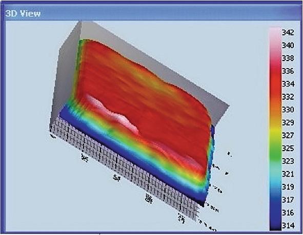
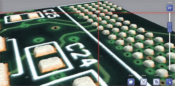
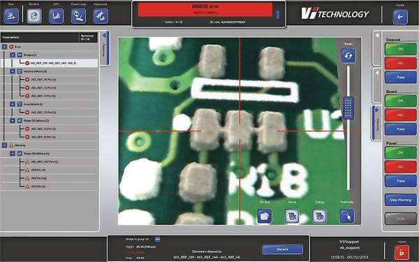
Anyone who has seen a 3D SPI system will be familiar with the typical topographic presentation of detected defects. The displays give a representation of the profile of a particular pad. However as they are of a very small area, they can be difficult to relate to the area of the PCB. An alternative solution offers large true 3D image of the area surrounding the particular pad, showing also the texture of the surface. This gives a far better representation of the situation. Both 2D and topographic images of large area are also available if required. The large area view offers also the capability to monitor the overall performance on the PCB. The Pi review screen offering a simultaneous 2d and 3D view of the defect. The 3D view is zoom able and rotatable. A topographic view can selected instead of the 3D view if so required.
Conclusion
Pi 360° Moire provides a true 3D capability and introduces significant benefits to both the monitoring and control of the SPI process. The ease of use and simplification of the programming removes the dependency on the skill of the programmer, ensuring optimum performance every time. The clear presentation of the inspection data offers a much improved insight into the print process and facilitates easy review, as well as providing the basis for accurate feedback to correct the print process and the full review data for subsequent analysis.
SMT Hybrid Packaging
Booth 7-423
Share:


