Nowadays, consumer electronics cannot be imagined without miniaturization anymore. The devices’ variety of functions is ever-increasing, while production costs are being cut down. Optical sensors and minicameras use special microoptical elements with lenses made of an innovative, UV-curing optical material.
Delo Industrie Klebstoffe, Windach (Germany)
Mini 3D cameras (e. g. array cameras) for mobile phones, LED flash lights and 3D screens: High-tech products are conquering our everyday life, and the demand for innovative, mobile terminals is continuously on the rise. More functions in ever smaller and thinner devices are the key to the electronics manufacturers’ success and a distinct competitive edge. Simple, fast and cost-efficient are essentials in production. Therefore, the role that microoptics play in many functions is an increasingly important one as they are both highly efficient as well as small and light-weight. This is why they satisfy the high-tech manufacturers’ needs.
Wafer level technologies as a basis for microoptics
For the production of microoptics, wafer level technologies (WLT) have become established during the past ten years as they comprehensively satisfy the high-tech devices’ multifarious needs. On the one hand, WLT produces up to 4,000 objectives simultaneously and at low cost. The optical systems can directly be inserted into automated surface mounting machines (SMT machines), and soldered afterwards. This simplifies and accelerates the entire production process for a mobile phone. On the other hand, this technology is scalable and therefore promotes the trends towards ever-small and thinner optics.
WLT produces up to 4000 objectives at the same time and low cost. The optical systems can directly be inserted into automated surface mounting machines (SMT machines), and soldered afterwards. This simplifies and accelerates the entire production process for a mobile phone. In addition, this technology is scalable and therefore promotes the trend towards ever smaller and thinner optical elements.
Delo has developed a versatile range of new, light-curing materials with outstanding optical properties used for lens production in LED and camera applications. The Katiobond adhesive family is mainly characterized by minimal curing shrinkage, maximum optical quality, and dimensional stability upon thermal stress.
The challenges material suppliers are facing consist of optimizing and adapting the adhesive formulations so as to achieve sophisticated optical features including surface roughness < λ/10, very high transparency in the visible range and thermal resistance (soldering process at 260°C).
High transparency despite light and thermal influence
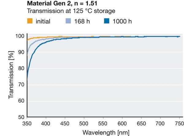
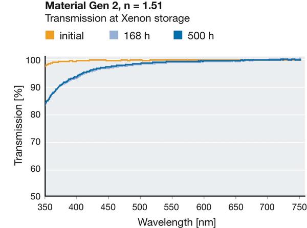
One key precondition for a functioning lens of UV-curing epoxy resin or acrylate is a consistently high transparency upon thermal and UV stress. This was achieved through intensive research and development as well as close collaboration with customers. Thermal and UV stress tests prove that the transmission at 400 nm and a layer thickness of 100µm always remains above 92 percent. Even during a thermal stress test at 120°C for 1,000 h, the new optical materials loose a maximum of 2 percent of their original transmission.
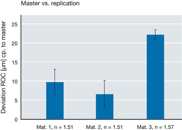
The material manufacturers’ requirements also include a very high optical quality of the adhesive. Comparing the surface roughness of the imprinted lens to that of the master lens with the help of a profilometer demonstrated that a high optical quality of < λ/10 is achieved.
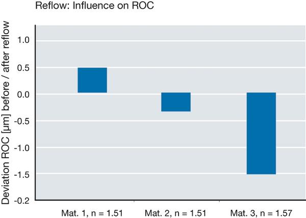
Over thermoplastic materials, such as PC or PMMA, the thermosetting imprint materials have the advantage of excellent thermal dimensional stability up to 260°C during reflow soldering processes. This is another important precondition for the adhesive being usable in standard mounting systems for optics manufacture.
Stamp is compatible with the optical material
To achieve high production volumes at low cost, automated processing must be possible, as well.
Lenses imprinted from optical materials were developed and individually optimized for various process, for example wafer lens imprinting with a stamp made of silicone, or LED lens replication by means of hard molding. Freedom from bubbles, repeated use of the stamps, and fast curing are essential for high machine output.
Basically, several thousand lenses can be replicated from one master lens through multiple stamp imprinting processes. For economical reasons, infrequent exchange res. longevity of the stamp in production are necessary. Therefore, the stamp material must be compatible with the optical material – it should not or only hardly react with the stamp. The Katiobond OM adhesives have been optimized in such a way that the interaction with a silicone stamp (PDMS) is only minimal.
In order to reduce chromatic aberrations of the lens and diminish the challenges, for example in the production of high-performance Fresnel lenses, DELO’s product range covers a wide range of refractive indices (n = 1.51 – 1.60) and Abbe numbers (Abbe = 27 – 54).
Perfect alignment of microoptics to the optical axis
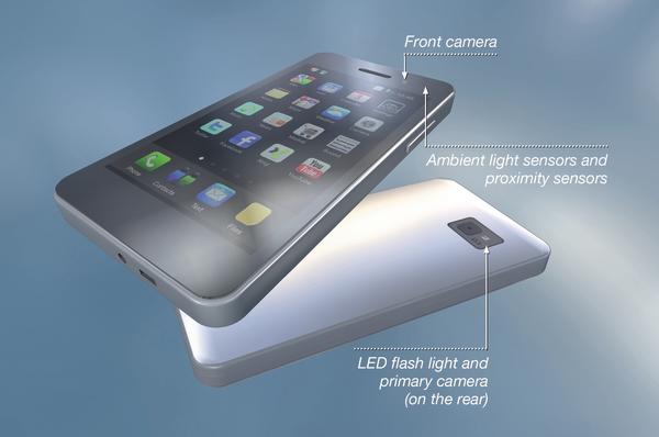
When producing minicameras, LED flash lights or proximity sensors, the microoptical elements must be separated, sawn, and then aligned to the optical axis. For the utmost precision, high output and, consequently, cost-efficient production, fast fixation after positioning of the optics on a substrates using a dual-curing adhesive is of great importance.
The optics are aligned as long as the adhesive is liquid. As soon as the optics have achieved their correct position, fast light fixation within seconds is required. Subsequently, the adhesive – mainly in shadowed areas – is completely heat-cured in just one curing step. In doing so, the temperature must not exceed 85 °C due to temperature-sensitive antireflective layers. The adhesive may shrink only slightly during final curing to reduce focus effects to a minimum.
Specifications of machine constructors1 show an alignment precision of 3s <±5um (XYZ) and an incline of ±0.1°. Typical applications include active alignment processes used in the production of compact camera modules.
New Dualbond adhesives have been optimized specifically for these applications, and are characterized by low water absorption and low shrinkage. The adhesives retain their features even during temperature stress.
To choose the perfect material for a certain task, the end user and application experts must collaborate closely so that the adhesive can ideally be adjusted to the requirements on viscosity, flow behavior and dispensing properties. Thus, the customers are enabled to produce their innovations in a fast and uncomplicated way using various processes, and push new developments.
About Delo:
The company is a leading manufacturer of industrial adhesives with its headquarters in Windach near Munich, Germany. In the past financial year 350 employees generated sales revenues of EUR 51.7 million until March 31, 2013. The company supplies tailor-made special adhesives and complementary equipment for applications in special lines of business – from electronics to the chip card and automotive industry, as well as in glass and plastic design. The customers of the company include Bosch, Daimler, Festo, Infineon, Knowles and Siemens. Delo has a network of worldwide distributors and sales partners.
Zusammenfassung
Miniaturisierung ist aus dem Bereich Konsumer Elektronik heute nicht mehr wegzudenken. Die Funktionen in den Geräten steigen, während die Kosten in der Produktion sinken. Für optische Sensoren und Minikameras werden hierfür spezielle Mikrooptiken mit Linsen aus einem innovativen, UV-härtenden optischen Material eingesetzt.
On ne peut plus s’imaginer l’électronique grand public sans miniaturisation. Les fonctions des appareils ne cessent de s’élargir tandis que les frais de production diminuent. Des microoptiques spéciales dotées de lentilles en une matière optique innovante durcissant aux UV sont utilisées pour les capteurs optiques et les minicaméras.
Share:


