Corrosion of electroless nickel/immersion gold plated surfaces is known as the black pad effect. This designation can be traced back to the appearance of this particular type of corrosion – gray to black areas on the pad surface which are very difficult, or in some cases impossible to solder. The black pad effect always results in mechanical weakening of the solder joint, and sometimes to complete failure due to separation of the solder joint from the pad.
Dr. Hans Bell, Rehm Thermal Systems, Blaubeuren-Seissen (Germany)
Black pad can be disastrous because the defect can’t be detected by means of simple visual inspection before assembling the PCB, and initially results in normally formed solder joints while soldering the pad to be wetted. The defect is not detected until an in-circuit test is conducted or the PCB fails in the field. Frequently, only a few of the PCB’s pads demonstrate the black pad effect.
Importance of the material
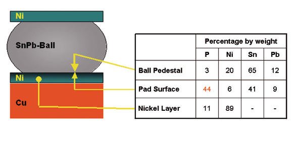
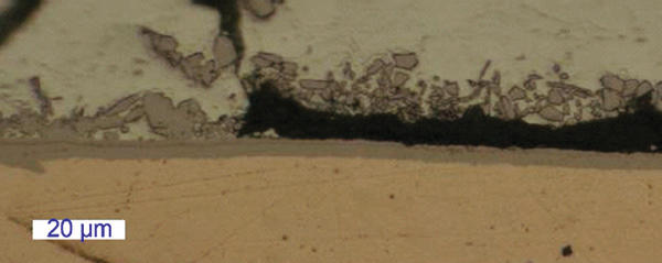
The black pad effect can be identified on the basis of abnormally thick layers with high phosphorus content on the nickel. A large portion of the failures shown in the micrograph are caused by an open joint between the nickel-tin intermetallic zone (Ni/Sn IMZ) and the nickel layer (EN). In some cases, a gray-black layer with high phosphorus content between the Ni/Sn IMZ and the nickel layer has been substantiated instead of a distinctly open joint.
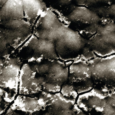
ENIG surfaces which demonstrate the black pad effect have a scaly appearance when viewed under an electron microscope, which are reminiscent of a dried out mud puddle and are thus known as “mud cracked surfaces”. According to Mei et al. [2.34], this scaly appearance is the result of a galvanic corrosion attack on the nickel layer during gold deposition. In the case of electroless deposition of nickel layers to copper, phosphorus is also incorporated into the nickel layer as a result of the chemical process. Phosphorus content typically lies within a range of 7% to 11%.
According to Biunno [2.36], if too little phosphorus is deposited along with the nickel, the resistance of the resulting layer to acid corrosion is too low. As a consequence, too much nickel is dissolved during gold deposition in the acidic gold immersion bath, and a layer which is rich in phosphorus forms underneath the gold layer. With a layer thickness of less than 3µm and a phosphorus content of less than 6% by volume, the nickel layer becomes more susceptible to corrosion.
However, if nickel is deposited with an excessive phosphorus content, readily solderable surfaces are obtained, but they are less resistant to thermo-mechanical stress. The reason for this is the fact that phosphorous does not participate in the formation of the intermetallic phase during soldering (in this case NiSn IMP), which leads to an accumulation of phosphorous on the surface of the nickel layer. According to measurements performed by Champaign et al. [2.37], the phosphorous content of a layer of this sort amounts to 17.4% by weight in the in black pad area, whereas only 7.4% by weight was measured in the uneffected nickel layer. These results also confirm EDS measurements performed by Bulwith et al. [2.38]. Each additional exposure to thermal stressing, for example in reflow or wave soldering, causes further growth of this layer and resultant weakening.
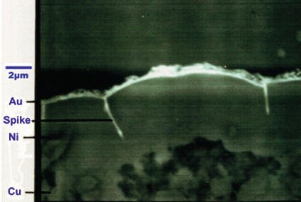
The black pad effect was observed by Snugovsky et al.[2.39] after soldering with SnPb, as well as after lead-free soldering. In particular in the case of excessively thick immersion gold layers (0.18 to 0.37µm), highly corroded Ni layers were substantiated. So-called corrosion spikes can frequently be observed in micrographs, which penetrate the entire nickel layer and are enriched with gold. These spikes provide the solder with a path by means of which direct contact can be established with the base copper, and allow for the formation of copper-tin intermetallic phases. Nickel-rich intermetallic phases are formed within the corroded Ni layer, and produce a mixture of Ni3Sn and Ni3P phases. At the same time, Me3Sn4 phases (Ni3Sn4, (Au,Ni)Sn4, (Ni,Cu)3Sn4) are deposited at the boundary layer adjacent to the solder. Adhesion between the nickel-rich phases and the (metallic)3Sn4 phase is poor, which makes it very easy for cracks to occur at these boundary layers.
Higher reflow temperatures are incapable of preventing the formation of black pads.
Which measures can be implemented in the mid-term in order to avoid failures due to the black pad effect?
- The best advice is to reject the delivered manufacturing lot of PCBs.
- Significantly shortening time above liquidus and reducing the maximum temperature of the soldering process is less advisable.
In the long-term, PCB manufacturers will have to implement measures which make it possible to better control deposition parameters (phosphorous content, pH value etc.) during the production of ENIG surfaces. In addition to good bath monitoring, Schmidt [2.33] recommends limiting bath age to no more than six MTOs (metal turnovers). The phosphorous content on the nickel layer should amount to roughly 8% to 10%, and the thickness of the gold layer should lie within a range of 80 to 150nm.
Zusammenfassung
Der Auszug aus dem Buch „Grundlagen des Reflowlötens, Teil 1“ von Dr. Hans Bell befasst sich mit dem Black-Pad-Effekt, welcher stets zu einer mechanischen Schwächung der Lötstelle und gelegentlich auch zum Totalausfall durch Trennung der Lötstelle vom Pad, führt.
L’extrait tiré du livre „Règles de base pour la soudure Reflow, Partie 1“ du Dr. Hans Bell traite de l’effet Black-Pad qui entraine toujours un affaiblissement mécanique du point de soudure et peut également engendrer occasionnellement une panne totale par le détachement du point de soudure du Pad.
Literature:
[2.33] Ralf Schmidt, Charakterisierung von Leiterplattenoberflächen, Proceedings OTTI Weichlöten, 20.-21.10.08 Würzburg
[2.34] Z. Mei, P. Johnson, M. Kaufmann, The effect of electroless Ni / immersion Au plating parameters on PBGA solder joint attachment reliability, IPC National Conference Proceedings: A summit on PWB surface finishes and solderability, September 22–23, 1998 Austin Texas, pp 19 – 42
[2.35] P. Snugovsky / Celestica Inc., 2002
[2.36] N. Biunno, A root cause failure mechanism for solder joint integrity of electroless nickel / immersion gold surface finishes, SMTA October 12–16, 1999
[2.37] Robert F. Champaign, Jodi A. Roepsch, Marlin R. Downey, Afraid of the dark, Circuits Assembly, January 2004, pp. 22 – 25
[2.38] Ronald A. Bulwith, Michael Trosky, Louis M. Picchione, Darlene Hug, The Black-Pad failure mechanism – from beginning to end, Global SMT & Packaging, pp. 9 –13
[2.39] P. Snugovsky, M. Kella, Z. Bagheri, M. Romansky Lead-free and lead-bearing solder intermetallic formation on electroless Ni / Immersion Au interconnects affected by Black-Pad, APEX 2002, proceedings of the technical conference, San Diego, January 19–24, pp.S02–1
Share:


