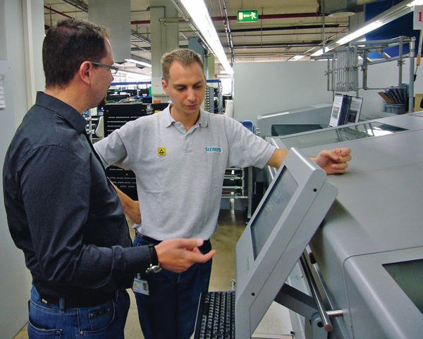
Siemens AG is a leading global electronics and electro-technology concern. 430,000 employees develop and manufacture products and produce systems and equipment for tailor-made solutions. The Volketswil plant, which is part of the Fire and Safety & Security Products (FS) business unit’s Building Technologies division, produces innovative fire protection components. Since the beginning of 2009, the Volketswil plant has been collaborating with Kirsten Soldering AG in the field of Through Hole Technology (THT).
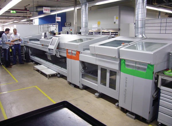
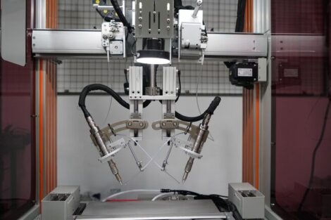
With its new Modula Wave wave soldering system, Kirsten Soldering AG has produced a major prerequisite for a high-quality, energy-saving soldering system. The compact design means that Siemens is able to set up the Modula Wave on its production line in a very cost-effective and space-saving manner. The modular design played an important part in this regard. No specialised amendments of transport and no alterations to the building were necessary to transport and install the system in the production facilitie. Each module (W x D x H: 750 x 1500 x 1500 mm) was transported individually and could there- fore be conveyed to upper storeys in a nor- mal lift or through smaller gates without problems.
Considerable cost savings
This stands for considerable cost savings compared to conventional systems. The system was configured precisely to our requirements. New components such as additional pre-heating modules can be integrated into the existing system very quickly and simply should these requirements change in the future. This is also possible at any time even after the system has been operated for a certain period of time. The initial investment could be kept low, and the system can be expanded by adding modules at any time if production requirements and additional products demand it. The modules are always constructed according to the same principle and are then simply placed next to each other, aligned and bolted together on the production line. The system is also deliberately designed with a limited range of parts and components. This, of course, simplifies preventive maintenance for staff and keeps the cost of storing replacement parts low.
Attention has also been paid to an energy-efficient design. The solder pot is compact und the soldering pump works according to the stator/rotor principle and thus does without a single moving part. The only thing that moves is the solder. All wearing parts which can cause problems in conventional soldering pumps are therefore immediately dispensed with. For this reason, the Kirsten Jet Wave also needs a significant smaller solder bath than conventio- nal soldering pumps does (just 60 kg). The results are substantially lower energy consumption and a short heating-up time of just one hour.
Lower consumption of solder
The low content of the solder pot means that the cost of the capital tied up in solder is also significant lower. One complete filling of the solder pot costs only a fraction of what it does bevor. The formation of waste metal is mini-mised by the compact solder pot and the resulting small, unprotected solder surface which also means that solder consumption is kept low. A very high solder turnover ratio is achieved with a capacity of just 60 kg of solder, which also reduces contamination of the solder bath to an absolute minimum. If the contents of the solder pot still have to be changed, the costs of refilling new solder are minimal.
The system is operated with partial gas treatment with nitrogen in the critical range. The solder pot is covered by a nitrogen hood as far as possible. Nitrogen is blown in through sintered pipes at critical points (directly at the wave outlet, below the hollow shaft at the solder discharge and above the solder bath) by means of the wave, and a residual oxygen quantity of 20 to 150 ppm is achieved during the soldering process. This forms a high-quality solder joint. Consistent wave geometry is also guaranteed and waste metal is prevented from forming to a large extent. Consumption is relatively low at approximately 15 m³/h, meaning a good cost-benefit ratio.
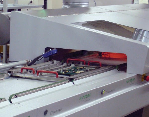
The soldering wave is formed through channels and the neck of the jet via a 1.3 mm wide jet in a soft and smooth counter-direction jet hollow wave. This principle allows waves of different heights to be created just millimetres apart up to a height of approximately 35 mm. This always permits optimum adjustment of the wave height for a wide variety of applications. In this way, the wave also reaches problem areas such as soldering pads in deep pockets when covering SMD or plastic components with the assistance of a mask. In this process, the soldering pads are washed with solder from a relatively large distance and not dragged through a slowly flowing wave (delta wave) as with most soldering systems. For this reason, it is also not necessary to convey the components through the wave by an angled transport system. Another reason for the compact design of the Modula Wave is the horizontal transport through the entire system; that means there is a uniform transport height and no upward or downward sloping ramps to reach an initial level again.
Preventing solder bridges
With the high flow rate of 0.8 m/s the hollow wave achieves optimum circulation for soldering glued SMD components on the underside, thus preventing solder bridges from forming. The drag resulting from the Bernoulli Effect makes the mechanical pressing of the circuit boards over and above their own weight unnecessary.
A point which is just as decisive for quality is the gentle treatment of the circuit boards. Thanks to the adjustable contact time, they are only subjected to a very low thermal load. This means little stress for circuit boards and components. A further plus with the Modula Wave is the quickly replaceable, wheel-mounted moveable solder cart. A second solder cart with a different solder alloy, such as leaded solder, is pre-heated to a certain temperature below the melting point in a separate docking station and the system can then, for example, be converted from lead-free to leaded soldering material (or vice versa). Long waiting times for cooling down and reheating and expensive standstill times are convincingly reduced in this way.
Moreover, service and adjustments can be carried out on the second soldering module in the docking station without interrupting production. The simple design of the individual modules permits good access to individual components. These are the right prerequisites for preventive maintenance. Worn or faulty parts can thus be replaced with little time and effort.
The fluxer unit, which must be regularly preventively cleaned to ensure uninterrupted and safe flux application, can be removed from the fluxer model in just a few seconds by means of quick-release closures for the controller, flux supply, and pressurised air and a simple drawer construction. All important locations can then be easily cleaned and serviced on a table, and the system is ready for operation again in a very short period of time. If the standstill time needs to be minimised even further, it is possible to work with a second fluxer unit. This can be changed within one minute and the contaminated unit can then be cleaned unhurriedly and prepared for the next deployment during production.
Operating is very simple
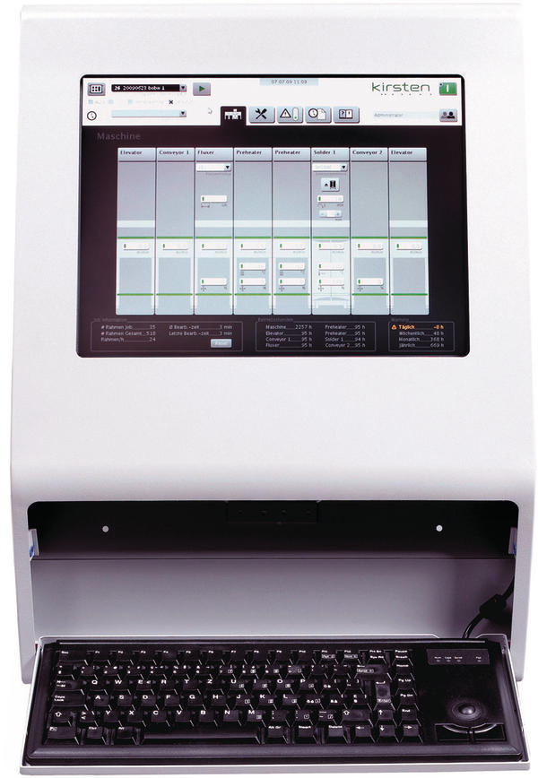
Operating the system by the Visko user interface is very simple. The individual programmes are automatically initialised with all critical parameters by RFID system. Deviations are reported immediately both optically and acoustically. All values for the process steps run through are saved in log files and can be accessed at any time for quality management-relevant information. The error rate of the processed circuit boards has been improved since the deployment of the Kirsten system. Special mention should also be made of the excellent customer service which Kirsten Soldering guarantees. Company-specific requirements and additional software wishes were positively received and realised. The following factors were of special significance for the choice of this wave soldering system for the Siemens’s Volketswil location: investment level, operating costs, low mainte-nance, low energy requirements and high variant flexibility
SMT/Hybrid/Packaging Booth 7-219
Zusammenfassung
Siemens entwickelt und produziert weltweit eine Vielzahl von Produkten und Lösungen. Das Werk in Volketswil ist spezialisiert auf Produkte für die Feuerschutz- und Sicherheitstechnik des Geschäftsbereichs Building Technologies. Seit 2009 arbeitet das Werk mit Kirsten beim Wellenlöten bedrahteter Bauelemente zusammen.
Les 430 000 collaborateurs de Siemens AG développent et produisent une grande variété de produits et de solutions sur mesure dans le monde entier. Le site de Volketswil s’est spécialisé dans la production de techniques de protection incendie et de sécurité pour la division Building Technologies. Depuis 2009, ce site suisse travaille en collaboration avec Kirsten pour le soudage à la vague de composants câblés.
Share:


