Continuously enhanced technologies and production methods have upgraded RFID applications (RFID = radio frequency identification) from a niche article into a matter of the consumers’ everyday life. RFID is increasingly taking over the task of the previously ubiquitous barcode. Mainly logistics companies benefit from a considerable acceleration and facilitation of stock management.
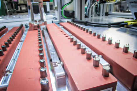
The demand for smart labels will rapidly increase in the near future as the entire value and production chain will be displayed though RFID and low-price products will be equipped with the respective labels on the medium term. In 2007, 144 million RFID tags were sold in the EU alone. According to a current study of the EU project „Building Radio Frequency Identification for the Global Environment“, this figure shall have increased to 90 billion in 15 years, resulting in a further expansion of RFID applications in different value chains. The information saved on the chip can be read or complemented by further data without contact by means of radio waves. An orientation of the label towards a scanner system is omitted: The individual piece goods of an entire pallet can be read in bulk and clearly identified as being original by means of the serial number of the chip. An appropriate system integration enables companies to have a detailed automatic overview of their current stock at any time as automatic booking-in and booking-out of the goods is ensured. This procedure is allowed by the use of a so-called smart label – a label with semiconductor chip and antenna – which communicates with the readers in the surrounding. Normally, the data of a smart label are transmitted in the HF (high frequency; 13.56 MHz) or UHF ultra high frequency, 860 to 930 MHz) range.
At the moment, manufacturers of semiconductors are in the focus as the chip has been the greatest expense factor so far. However, also the manufacturers of inlays and labels are coming under growing pressure to lower the unit costs for smart labels through optimized production methods and reduced expenses. One decisive and essential production step is the bonding of the RFID chip to the transponder antenna. On the one hand, this connection ensures the electrical contacting permanently (only that way, communication is enabled); on the other hand, this step essentially contributes to a highest possible yield in volume production. Due to the reliable connecting of semiconductor and antenna in seconds, so-called NCA (non-conductive adhesives) and ACA (anisotropic conductive adhesives) adhesives provide for an effective solution which is already successfully applied in millions of smart label units.
From COB process to flip-chip technology
The so-called COB (chip on board) and COF (chip on flex) technology represented the preferred method for the mechanical and electrical connection of semiconductor chip and substrate for numerous applications in the smart label sector and, initially, also for smart labels. During this process, the chip is mechanically fixed to a substrate and electrically contacted with gold wires in a so-called wire bond process. The individual contact areas must be processed successively. Afterwards, the contacts are protected against environmental influence by encapsulating the chip and the wires. Standard encapsulation compounds are cured by light or heat. Their curing times range from 30 seconds to 2 hours at temperatures from room temperature to 200 °C. For the bonding of bare semiconductor chips in smart label applications, however, this complex and relatively slow process is not an adequate solution. Considering the long curing times, the production of several billions of RFID labels per year would be unthinkable.
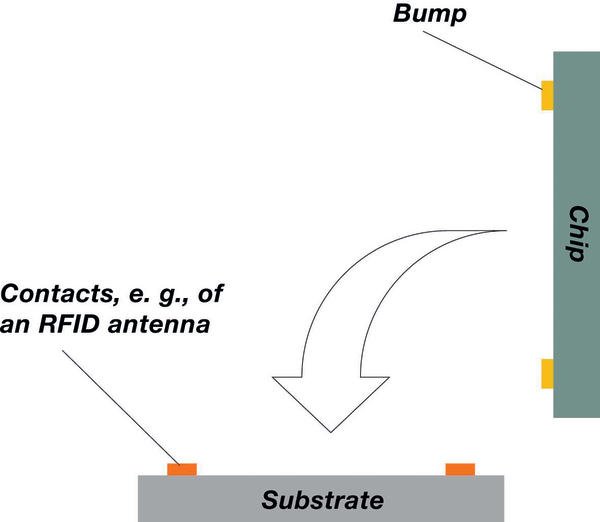
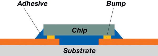
Here, the advantages of flip-chip technology come into play, enabling an easy, cost-saving and fast bonding of chips to different substrates. During the flip-chip process, the manufacturer equips the structured, active side of the semiconductor chip with so-called bumps. For establishing the contact, the chip which was refined with bumps is pressed into the substrate metallization with its active side facing the substrate (see figure 2 a). In theory, any number of electrical contacts can be established in one process step. The adhesive, which was pre-applied onto the active areas, can be cured by means of a heated stamp (thermode) during placement of the flip-chip. Thus, the chip is mechanically fixed and electrically contacted in only one process step. The contact areas are already protected through embedding them in adhesive (see figure 2 b).
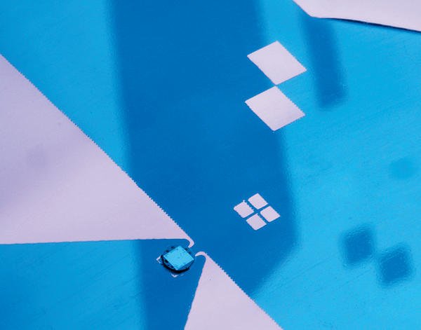
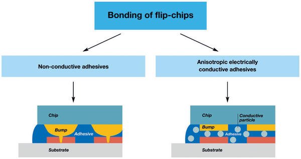
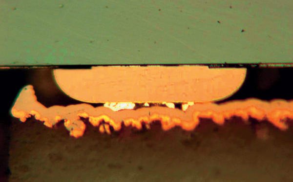
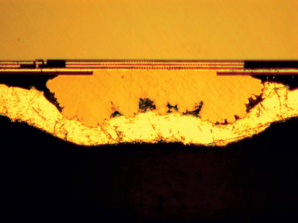
The decision on using an NCA or ACA depends on the available bump variants of the chip (see figure 3). Normally, ACA adhesives are preferred for very flat and even bumps (Ni/Au, Au). NCA adhesives are suitable for the geometrically irregular stud bumps or palladium bumps. Depending on the substrate base material (PET, paper, PI) and/or metallization (Cu, Al, Ag), accordingly tailored, one-component epoxy resins are used. Figure 3 shows the schematic setup of a flip-chip connection with non-conductive and anisotropic conductive adhesives. The adhesive is applied over all contacts without creating short circuits. Therefore, it completes the task of mechanical anchoring and permanent electrical contacting in one process step. Adjusting the particle content and the particle size to the application is decisive for the reliable contacting with anisotropic conductive adhesives. Basically, a sufficient number of particles must be present in the bump area to allow for the requirements on the reliability of the total system. The rule of thumb in the industry is that more than 10 particles must be between bump and antenna metallization. Moreover, different particle sizes are available to come up to morphological differences in the surfaces of the substrates to be bonded. The size of the particles used ranges from approx. 5 up to 20 µm in special applications. It can be seen in figure 4 that the electrical contact to the antenna is provided by the filler when using Au or Ni / Au bumps. The electrical conductivity of the bonded connection is brought about as soon as the adhesive and the conductive particles in it are being clamped between two contact areas. As this system is contacted in only one spatial direction (z axis), the adhesive is called anisotropic. The NCA adhesives are not equipped with fillers. The rough bump surface penetrating into the metallization layer generates the contact. The adhesive fixes the chip in this position permanently and ensures that the connection is reliably maintained during the lifetime of the inlay (see figure 5).
Fast curing and short cycle times
Until now, there is no generally valid specification for smart labels. The requirements on the performance and lifetime are adjusted according to the application. However, some basic requirements the bonded connection should meet can be stated:
- Depending on substrate and equipment, curing at 170 to 190 °C at the adhesive in 6 to 10 seconds
- Availability of ACA and NCA products for different chip and bump types
- Preferable universal adhesion to different antenna
- Resistance of the contacting during storage at 85 °C and 85 % relative humidity; temperature change tests from – 40 to + 85 °C; bending test (bending of the smart label over a radius of 2 cm) and permanent temperature storage at – 40 °C and / or 85 °C
In practice, reliability tests, e. g., humidity and long-term temperature tests with storage times of 168 to 500 hours and temperature change tests with 50 to 500 cycles are often required. Besides the ACA/NCA adhesive used, the performance of the substrate material is decisive for the reliability of the flip-chip bonding. Driven by cost pressure, this RFID market segment is developing rapidly. The standard antennas are mostly produced on PET foils or paper reels through different processes (etching, electroplating, printing processes, PVD). The quality and the surface properties can vary significantly from manufacturer to manufacturer. Therefore, it also has direct influence on the total performance of the smart label.
From theory to practice
To ensure permanent process stability and high reliability, several adhesives were being subjected to numerous examinations and investigations in the present test series. Here, the performance of two adhesives – anisotropic conductive, heat-curing epoxy resins with partly differing properties – is to be shown exemplarily. Moreover, further standard and development products with similar properties are available as NCA variants. The extractable ion content (Na+, K+, CI-, F-) of the adhesives tested is below 10 ppm and their water absorption is 0.4 %. The curing time of Delo-Monopox AC 265 (Adhesive No. 1) is 8 s at 190 °C with a thermode. Delo-Monopox AC VE 42878 (Adhesive No. 2) is cured at 180 °C for 6 s. The storage life at 5 °C of adhesive No. 1 is six months and of Adhesive No. 2 four months. Also the storage life at room temperature (20 to 25 °C) of Adhesive No. 2, which is one week, is slightly lower than that of Adhesive No. 1, which is two weeks. For the tests described, PET substrates with aluminum metallization were used. A silicon semiconductor with Au bumps and test structure for the resistance determination was selected as chip.
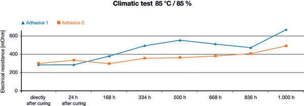
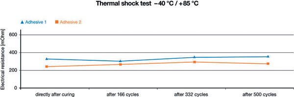
The following shear strengths were determined for a chip with an area of 1 x 1 mm². The tests were carried out with a die shear tester of company DAGE according to Delo Standard 30. This standard, which was specifically developed for this purpose by Delo, is used for the determination of the shear strength of mainly die attach adhesives and the comparing evaluation of their shear strength. The shear strength on PET / Al of Delo-Monopox AC 265 is 23 N and of Delo-Monopox AC VE 42878 already 25 N. The high strengths reached guarantee an excellent mechanical anchorage of the chip and, therefore, form the starting point for successful temperature and humidity storages. Here, storage at 85 °C and 85 % relative humidity proved to be the most critical reliability test as adhesive properties such as low humidity absorption, high adhesion, low subsurface migration tendency on the relevant substrate and high strengths are especially stressed in this test (figure 6). Moreover, the behavior at temperature changes is decisive for the practical use. Having a glance at RFID applications in goods and vehicle traffic with different ambient conditions, this becomes quite clear. Here, temperature ranges of – 40 °C to + 85 °C emerged as relevant for the application (figure 7).
Stress relaxation
During both tests, an excellent performance of the ACA products could be observed. The slight increases in the resistance values after temperature shock and humidity storage can primarily be attributed to substrate aging, i. e., oxidation of the antenna metallization, swelling effects in the base material and a marginal relaxation of the adhesive in the first hours of the storage tests. Practice showed that these moderate changes of resistance do not carry weight for HF and UHF applications.
Conclusion
NCA and ACA products make it possible to maintain extremely short cycle times and, therefore, to reach extremely high throughputs. More than 10,000 UPH have become possible for smart label applications, depending on substrate dimensions and flip-chip mounter. At the same time, the flip-chip method allows for the call of efficiency, i. e., in the meantime, up to 20 million chips can be contacted with one kilogram of adhesive. Therefore, the NCA/ACA products present the most efficient method for the contacting of chip and substrate. Due to the high reachable reliabilities in the field of the manufacturing process and the lifetime, the systems produced with NCA/ACA adhesives offer a stable and efficient way in the production of RFID labels.
EPP Europe 463
zusammenfassung
NCA- und ACA-Klebstoffe bieten durch ihre sekundenschnelle und zuverlässige Verbindung von Halbleiterchip und Antenne eine effektive Lösung in der Smart-Label-Herstellung. So sind für Smart Label-Anwendungen, abhängig von Substratdimensionen und Flip-Chip Mounter über 10000 Uph möglich. Im Flip-Chip-Verfahren können pro Kilogramm Klebstoff bis zu 20 Mio. Chips kontaktiert werden.
Les colles NCA et ACA constituent une solution efficace dans le domaine de la fabrication d’étiquettes intelligentes, grâce à leur assemblage ultra-rapide et fiable d’une puce semi-conductrice et d’une antenne. Ainsi, pour les applications d’étiquettes intelligentes, plus de 10 000 Uph sont possibles en fonction des dimensions du substrat et du système d’assemblage Flip-chip. Le procédé Flip-chip permet de connecter jusqu’à 20 millions de puces par kilo de colle.
I collanti NCA e ACA offrono una soluzione efficace nella produzione smart label grazie al loro collegamento veloce e affidabile tra chip a semiconduttori e antenna. Pertanto per impieghi smart label sono possibili oltre 10000 UPH a seconda delle dimensioni del substrato e del Flip-Chip Mounter. Nel processo Flip-Chip possono essere collegati fino a 20 milioni di chip per ogni chilogrammo di collante.
Share:


 Florian Hierl and Dr. Michael Stumbeck, DELO Industrial Adhesives id=)