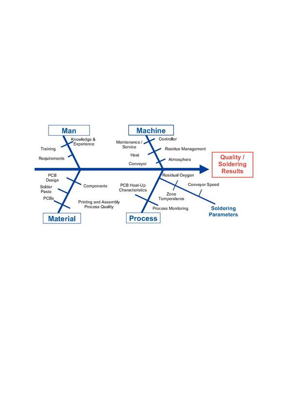
After creating an Ishikawa diagram (also known as a fishbone diagram) for the reflow process as shown in figure 1, a great variety of factors which influence the quality of the soldering results become apparent. The soldering parameters, i.e. the temperature zones set up in the reflow system, conveyor speed and the soldering atmosphere (air or nitrogen), are just one aspect in this complex mix of influencing factors. Nevertheless, the following question is frequently asked: “How do the parameters of the reflow system have to be changed in order to minimize the number of soldering defects (or the frequency of a certain defect), and what does the ideal reflow profile look like?”
Unfortunately there’s no simple answer. The mechanisms which contribute to the occurrence of soldering defects are subject to such a great variety of interactive parameters that changing a single manipulated variable will often have no effect at all. Or, in some cases, the frequency distribution of a given type of defect is simply changed. Just how difficult it can be to optimize a reflow profile is discussed in this article with the help of several examples. There is currently no generally applicable standard which points out limits for “good soldering”. The most commonly quoted standards, namely IPC/JEDEC J-STD 20 D (July 2004) and IEC 60068–2–58, do not describe how the PCB manufacturer should optimize his reflow profile. They simply indicate in accordance with which thermal loads moisture-sensitive components are to be qualified, to assure that they’re durable enough for a reflow process.
No generally applicable standard
Nevertheless, these standards indicate which limits need to be adhered to for reliable soldering. In IPC 20 D, the essential limit profile parameters for PCBs processed with tin-lead and lead-free solder are listed in table 5. However, when using these parameters it must never be forgotten that this standard is targeted at moisture sensitive components and their classification. For example, the lead-free process is specified with a time at liquidus of 60 to 150 seconds (tL). Leaving the solder in its molten state causes alloy formation effects and the formation of an inter-metallic phase which means that longer dwell times may impair the reliability of the solder joint. General experience indicates that a duration of 90 seconds at liquidus should not be significantly exceeded, which would of course be the case with a permissible limit value of 150 seconds in accordance with IPC 20 D.
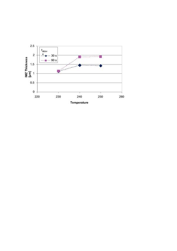
Examinations conducted by [3] (see figure 2) at SnAgCu solder joints reveal that extending soldering time from 30 to 90 seconds makes a greater contribution to the formation of an intermetallic phase than increasing soldering temperature from 240 to 250 °C. Each manufacturing facility is thus solely responsible for working out an ideal reflow profile for its products and the utilized materials (PCB, solder paste, components). And holistic thinking is always necessary in order to discover any weak points within the respective process.
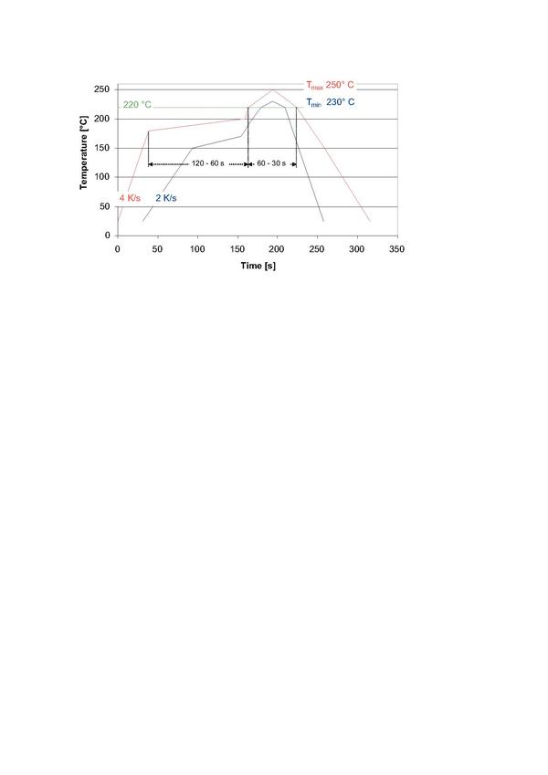
For example, a solder paste manufacturer recommends the temperature profile shown in figure 3 when using his SnAg3.0Cu0.5 paste.
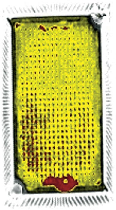
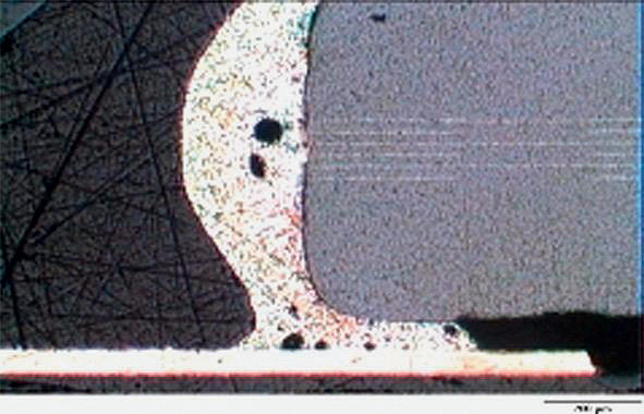
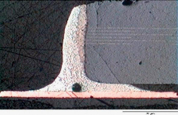
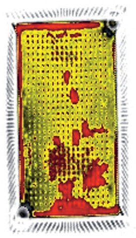
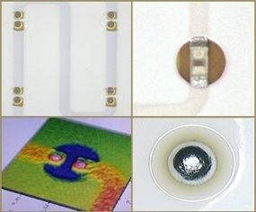
At first glance everything looks OK, but if processing of moisture-sensitive components is also taken into consideration we discover significant defects. According to IPC 20 D, a heat gradient of 4 K/s (which is permitted here as a limit gradient) is impermissible for moisture-sensitive components, and a temperature of 245 °C may not be exceeded at the surface of the packages of various large components (thickness > 1.6 mm, volume > 2000 cubic mm, see table 4–2 in IPC 20 D). If the requirements specified for the individual components are not complied with they may be damaged, for example delamination may occur as shown in the ultrasound image of the PFCM package in figure 4.
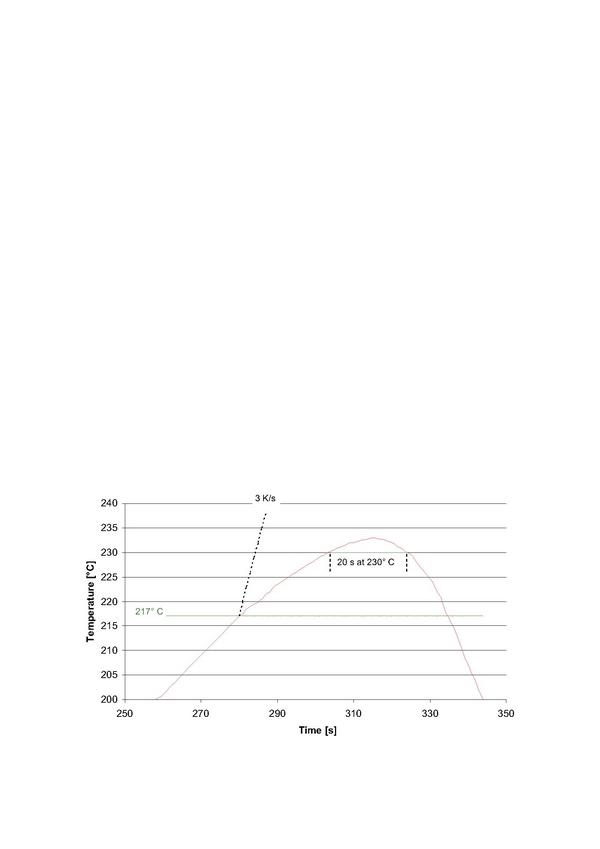
Maximum temperature in the reflow process is usually limited by the utilized components and materials. Minimum temperature is determined by the melting point of the selected alloy (217 °C for SnAgCu), as well as metallurgical necessary overheating. General experience indicates that overheating by approximately 10 Kelvin is sufficient. 20 seconds at 230 °C is recommended for the production of reliable solder joints in IEC TR 60068–2–580 (method for evaluating a possible lead-free reflow temperature profile).
Soldering temperature
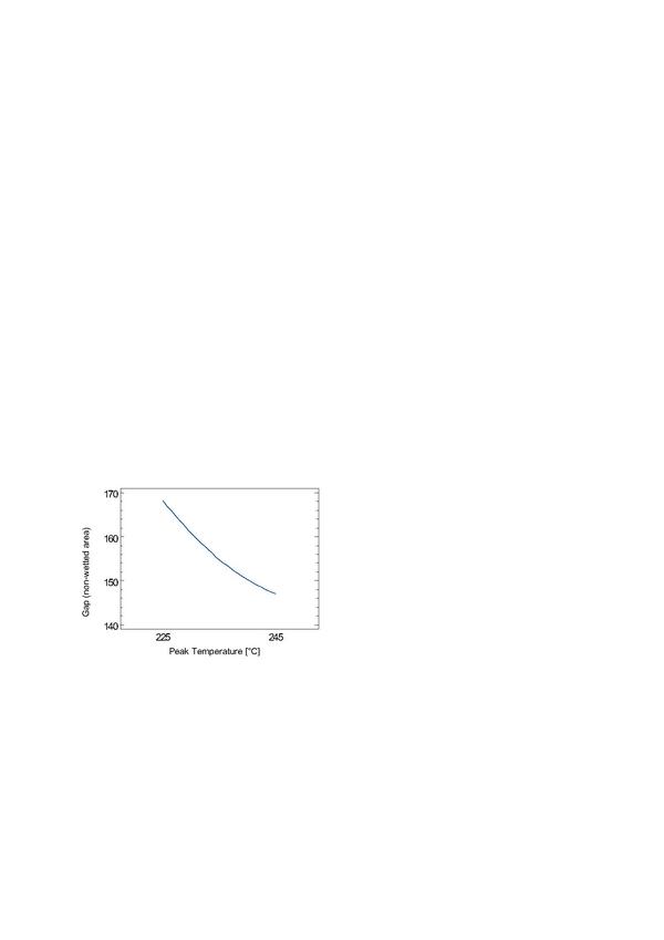
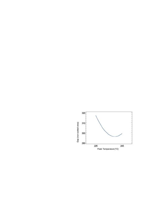
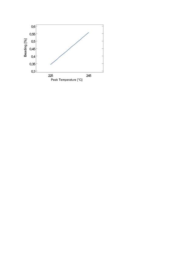
The higher the soldering temperature is, the more accelerated are diffusion and metallurgical interaction, which frequently has positive effects on wetting results. Figures 5a and 5b show that the non-wetted portion of the 0201 connector (gap) becomes significantly smaller, i.e. wetting is improved, as temperature is increased. Whereas increasing peak temperature improves wetting in this case, the number of beads may increase at the same time (figure 6). One possible explanation for this phenomenon might be the fact that the density and the viscosity of the liquid solder are decreased as the temperature rises. The component sinks down deeper due to gravitational force, and at the same time the capillary effect underneath the components is reduced as the height of the gap decreases.
Alleged poorer wetting is sometimes observed at silver-palladium plated components at high peak temperatures. The images shown in figure 7 depict the wetting results at two different peak temperatures. At 260° C, all of the solder is drawn to the connector, causing the formation of a convex solder joint with minimal spreading over the pad. The AgPd connector is so well wetted at the higher temperature that all of the solder is drawn upwards and there isn’t enough left to fully wet the NiAu pad on the PCB. If the temperatures are reduced, wetting times are generally extended resulting in the formation of a well-balanced, concave solder joint.
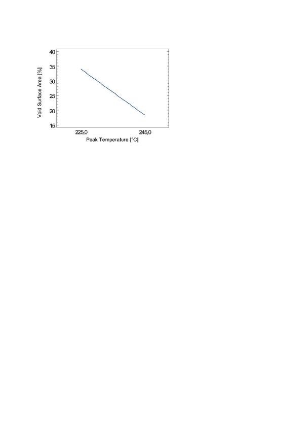
In contrast to this, voids in solder joints can be minimized by increasing the peak temperature (see figure 8). Increasing the temperature of the molten solder reduces its surface tension. This makes it easier for gasses trapped in the solder to escape. Thus there is no simple answer to the question of how the parameter must be changed in order to reduce the defects rate for the PCB. An evaluation must always be made in each individual, concrete case, and for the respective primary defect.
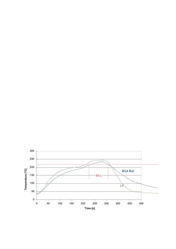
Temperature rise at the PCB is proportional to heat absorbed by the component, which in turn depends upon dwell time (determined by conveyor speed) and temperature within the reflow system. However, uniform flow of heat from the system to the PCB results in greatly varying temperature curves at the various solder joints. This is caused by varying thermal masses on the PCB. Figure 9 depicts a case of this sort.
The soldering temperature specified for the BGA ball, namely 235 °C, resulted in a time above liquidus of 60 seconds. However, due to the fact that the mass of the PCB was less at the point of measurement, time above liquidus was 90 seconds at a maximum temperature of 245 °C at this point. Longer dwell times at higher temperatures cause alloy formation effects and the formation of an inter-metallic phase. As a result, solder joints on actual PCBs differ with regard to their structures. Intermetallic phase formation can be described by means of the following equation:
Generally speaking, a time at liquidus within a range of 30 to 90 seconds is considered ideal, and in any case 120 seconds should not be exceeded and 20 seconds should not be fallen short of.
In their work with mixed assemblies (lead-free and lead containing), Grossmann et al [2] established the fact that uniform (homogenous) distribution of lead phases within the solder’s grain structure is achieved with a heat equivalent of less than 300 Ks.
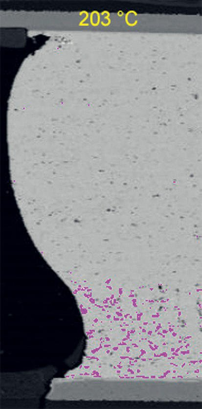
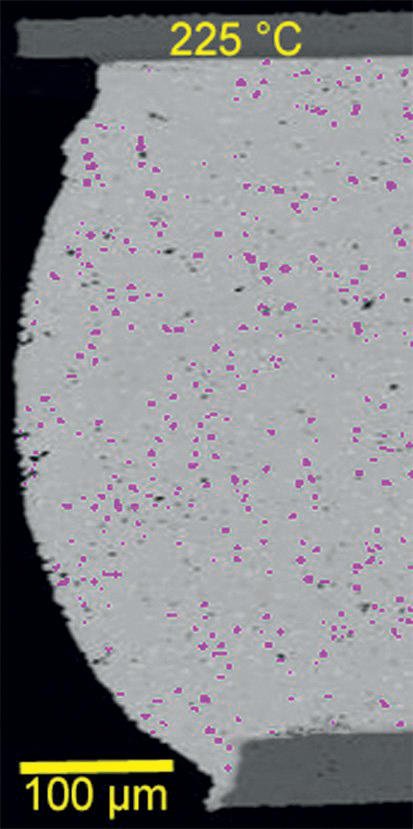
The micrographs in figure10 show an SnAgCu ball which was soldered with a lead-containing solder paste at low temperature (left), and at a temperature of 8 K above the melting point of the lead-free ball (right). The lead phases are magenta colored in the images. If the temperature is too low, the lead-free ball does not melt, and the utilized amount of energy is insufficient for a homogenous distribution of the phases throughout the grain structure.
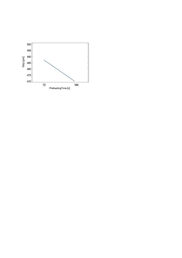
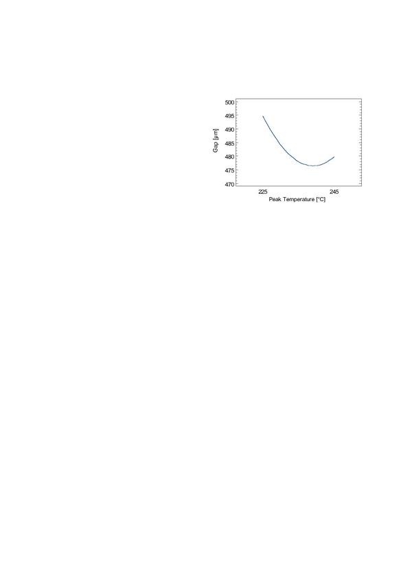
Beyond this, the BGA solder joint cannot collapse; the gap underneath the BGA is not reduced. Solder joints of this sort are less reliable. If concave warpage of the corners of the BGA is added to the other problems, an open is likely to occur. As maximum temperature and preheating time are increased (thus assuring better soaking), the gap underneath the BGA is significantly reduced (see figure 11).
The heat energy introduced to the solder joint is thus an important indicator for assessing reliability. The heat equivalent (QT) is calculated from the integral over the entire temperature sequence of the reflow curve:
QT = ∫ T (t) d t
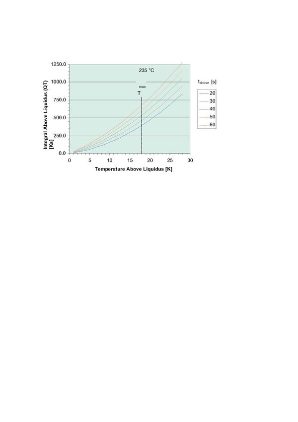
As shown in figure 12, the heat equivalent at liquidus is 550 Ks for the reflow curve recommended by IEC TR 60068–2–580.
The graph in figure 13 unites solder parameters and heat equivalent on the basis of metallurgical knowledge regarding the formation of a homogenous grain structure. With overheating to 10 K above liquidus, it’s apparent that the amount of heat required to exceed the QT minimum of 300 Ks is only introduced to the solder joint as of a dwell time of approximately 60 seconds. If the peak temperature is increased to the recommended level of 235 °C, adequate heat energy is also introduced for short soldering times.
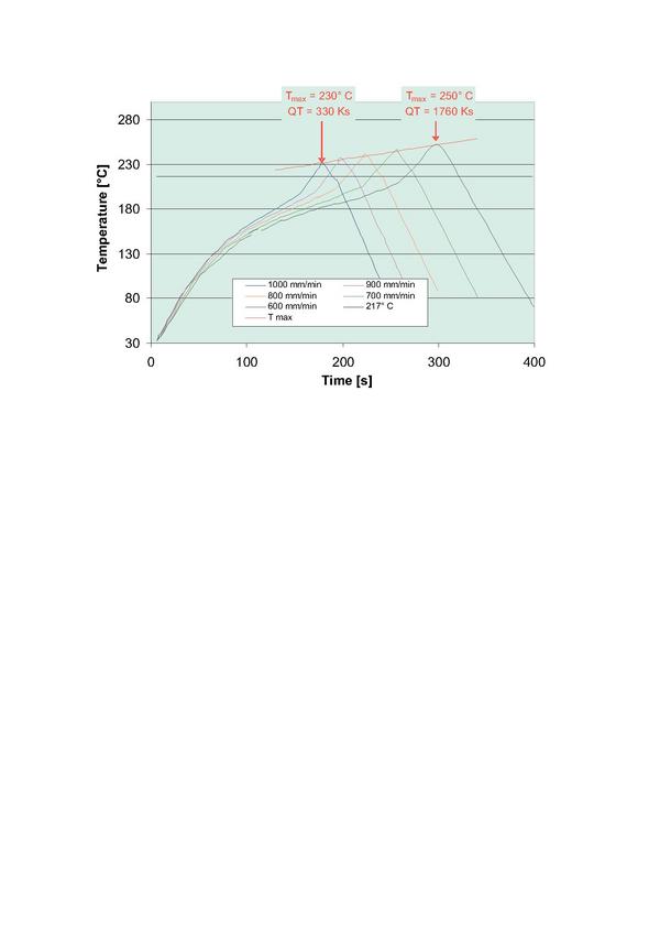
The soldering time of a reflow profile is determined primarily by the speed at which the PCB is transported through the reflow oven. Higher conveyor speeds result in shorter dwell times, and finally in excessively low temperatures at the PCB. Conveyor speed is therefore the most influential parameter for reflow profiling. As depicted in figure 14, increasing conveyor speed from 600 to 1000 mm per minute can increase the heat equivalent by a factor of 5.
In summing up general empirical experience and results included in the literature, we can say that 235 ± 5 °C is the ideal maximum temperature for the soldering process with SnAgCu.
Heat input into the PCB
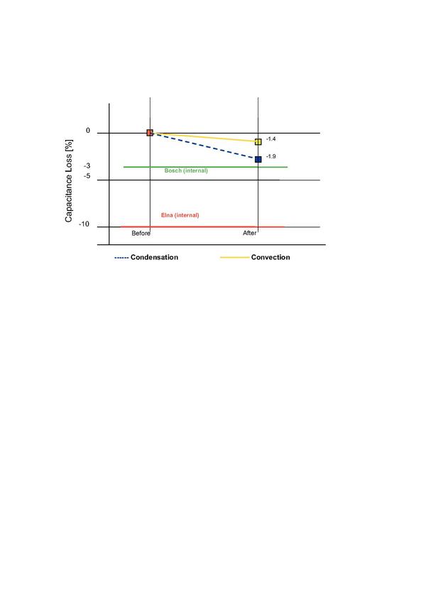
The fact that maximum temperature alone is not always decisive for the quality of overall results, but rather heat input into the PCB as well, is demonstrated by measurements at electrolytic capacitors after reflow with various soldering processes (see figure 15).
In the case of electrolytic capacitors, the comparably large amount of heat input achieved with condensation soldering (vapor phase soldering) leads to greater capacitance losses than after convection soldering.
Adequate soaking of the PCB can be very helpful during convection soldering, for example in order to prevent tombstones. Tombstoning depends upon the delay in wetting time between the right and left connector pads of a 2-pole component. The component rises at the side of the connector pad which is wetted first by the molten solder. Due to the fact that the thermal masses of the connector pads may deviate from each other significantly, adequate soaking of the PCB is required in order to homogenize temperature distribution. Increased dwell time in the reflow oven allows for heat conduction into the interior of the PCB, and thermal differences between the two connector pads are thus better equalized. The faster the PCB travels through the oven, the greater is the likelihood of tombstones, as is shown in figure 16.
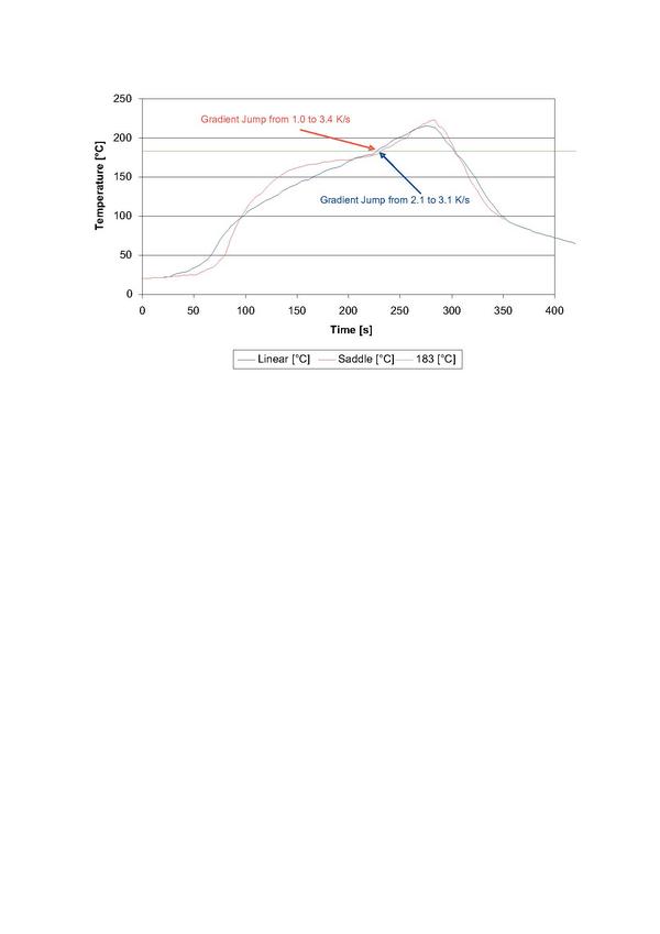
Heat equalization within the PCB becomes more and more difficult as heat gradients become steeper. For example, saddle shaped profiles often result in larger numbers of tombstones than is the case with linear reflow profiles. In the case of a saddle shaped profile, the gradient jump is more prominent at the transition to the solder’s molten phase, as can be seen in figure 17.
In the case of condensation soldering (vapor phase soldering), tombstoning may become problematic because up to ten times as much heat per unit of time may be introduced to the PCB due to the fact that the heat gradients are significantly greater. This can be remedied by reducing the heat gradients, as is possible, for example, with the Condenso injection process.
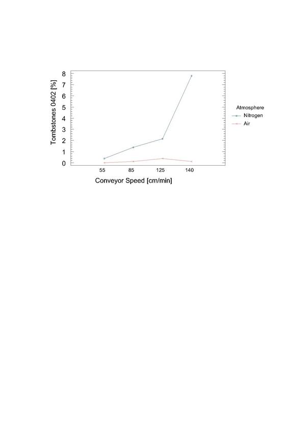
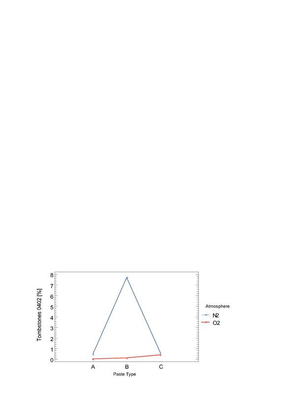
However, interactive influencing factors may lead to different results. For example, the number of tombstones rises as conveyor speed is increased in a nitrogen atmosphere, whereas it remains nearly constant in an air atmosphere.
Oxidation processes acting upon the surfaces to be wetted and the solder paste in an air atmosphere increase wetting time and thus reduce delay time between the right and left connectors. Pastes with adequately good wetting characteristics are capable of achieving equally low numbers of tombstones in a nitrogen atmosphere as is also the case in air (see figure 18).
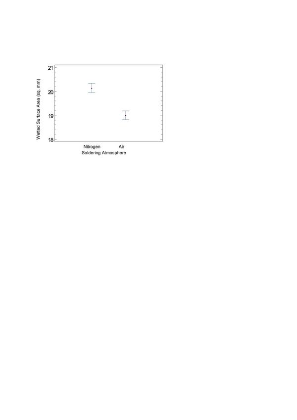
Whereas a nitrogen atmosphere may promote the occurrence of tombstones, it has a positive overall effect on wetting as is shown in figure 19.
The reduced wetting times achieved by means of soldering in a nitrogen atmosphere can also be taken advantage of in order to reduce the maximum soldering temperature in the reflow process. The is the decisive advantage offered by soldering in a nitrogen atmosphere.
As maximum temperature and overall heat input into the PCB are reduced, all of the utilized materials are stressed to a lesser extend during the reflow process.
Conclusion
This article demonstrates that highly complex interaction occurs during reflow soldering, and that for this reason there aren’t any simple solutions for problems with defects.
The requirements and limit parameters for all of the materials must always be taken into consideration in a holistic fashion, in order to create an ideal reflow profile.
Standards and specifications must not be used as dogmatic guidelines for temperature profiling, because they never take reliability demands placed upon the final product into consideration. Nevertheless, they do provide valuable information for setting up a robust reflow process.
SMT, Stand 7-329/NEW UK, B20, B30
EPP Europe 428
References
[1] H. Wohlrabe, T. Herzog, S. Schröder, Bericht zur Untersuchung des Einflusses von verschiedenen Löt- und Materialbedingungen auf die Qualität von gefertigten SMD-Baugruppen, TU Dresden 2007
[2] G. Grossmann, J. Tharian, P. Jud, U. Sennhauser, EMPA, Untersuchung der Mikrostruktur von blei-freien BGA-Anschlüssen, die mit Zinn-Blei-Lot verarbeitet worden sind, PLUS 8/2006
[3] Jianbiao Pan,Tzu-Chien Chou, Brian J. Toleno, Jasbir Bath, Effects of Reflow Profile and Thermal Shock on Intermetallic Compound Thickness for SnPb and SnAgCu Solder Joints, Proceedings APEX Feb. 2006, Los Angeles, CA
[4] Micrographs from: Johann Weber, Zollner, OTTI Regensburg 2000
[5] Images from Dr. F. W. Wulfert, 7. EE-Kolleg Sant Jordi März 2004
zusammenfassung
Es wird deutlich, dass beim Reflow-Löten eine komplexe Wechselwirkung stattfindet und dass es aus diesem Grund keine einfachen Lösungen für Probleme mit Defekten gibt. Zur Schaffung eines optimalen Reflow-Profils müssen die Anforderungen und Grenzparameter aller Materialien stets ganzheitlich berücksichtigt werden. Normen und Spezifikationen dürfen nicht als dogmatische Vorgabe für die Temperaturprofilerstellung angesehen werden, da sie nie die Ansprüche berücksichtigen, die an das Endprodukt in puncto Zuverlässigkeit gestellt werden. Dennoch liefern sie wertvolle Informationen zur Einrichtung eines stabilen Reflow-Prozesses.
Cet article démontre l’existence d’une interaction extrêmement complexe durant le brasage de refusion. Un phénomène qui explique l’absence de solutions simples en cas de défauts. Pour tous les matériaux, il convient d’adopter systématiquement une approche holistique des exigences et des paramètres limites, afin de créer un profil optimal de refusion. Les normes et spécifications ne doivent pas être utilisées comme des guides de caractère dogmatique. En effet, elles ne tiennent jamais compte des critères de fiabilité exigés du produit final. Elles procurent toutefois des informations de valeur pour la mise en place d’un processus robuste de brasage.
Il presente articolo dimostra come la saldatura a rifusione comporti delle interazioni estremamente complesse, per cui non esistono soluzioni semplici ai problemi dei difetti. Devono sempre essere presi in considerazione dal punto di vista olistico i requisiti e i parametri limite di tutti questi materiali, al fine di creare un profilo di rifusione ideale. Gli standard e le caratteristiche tecniche non devono essere assunti come direttive indiscutibili nella creazione di profili di temperatura, in quanto non considerano mai l’affidabilità richiesta per il prodotto finale. Tuttavia, offrono informazioni importanti per l’impotazione di un processo di rifusione robusto.
Share:


