Since the discovery of X-rays in 1895, X-ray technology has established itself in the electronics industry as a reliable means of detecting soldering defects and assembly errors. As technology advances, electronic assemblies and the components used in these assemblies are getting smaller and smaller, and often overlap each other on the two sides of the assembly creating challenging inspection requirements which for the most part can no longer be addressed by optical means. By using advanced X-ray systems not only the required high quality standards of manufactured products can be secured, but the complete production process can be monitored and optimized with real-time process control. In high-volume production such as in Automotive or Consumer Electronic applications, Automatic X-ray inspection (AXI) plays an important role to ensure the highest end product quality and reliability. Based on automated processes, x-ray technology has proved itself through precision, reliability, speed and minimal use of human labor. In the electronics industry, X-ray is mainly applied for inspecting solder joints as well as missing parts in completed assemblies or devices.
MatriX Technologies GmbH, Feldkirchen (Germany)
X-ray technology reliably detects typical errors such as solder bridges, drainage or incomplete melting of solder on components such as BGA, QFN, or THT that are not visually inspectable from the outside. Furthermore, the percentage of voids determines the quality and reliability of solder joints. In the following, the use of industrial x-ray technology will be explained based on three typical application examples: BGA ball inspection, PTH barrell-fill and QFN void inspection.
Inspection of Ball Grid Array solder joints
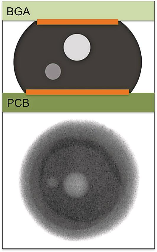
The following criteria determines the quality of soldered BGA components: solder bridges (shorts), offset/misalignment, missing or open solder joints, non-wetted balls and porosity. To assess misalignment, the grey value and thus contrast of the solder joints is considered. Because the pad appears brighter compared to the ball, the component offset can be measured from the degree of overlap of the two apparent circles. In a centrally positioned ball, the dark circle is located centrally within the bright circle.
For quite some time, a defect condition referred to as „Head-in-Pillow“ has gained increased attention on the manufacturing floor. It describes a solder condition, in which, although the pad is completely wetted with solder, the ball itself is insufficiently wetted. This condition is now safely detectable by appropriate picture settings and with the aid of special testing algorithms by using oblique x-ray image views (e.g. 45°). These non-wetted connections become clearly visible.
Pin Through Hole solder joints
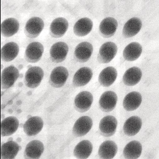
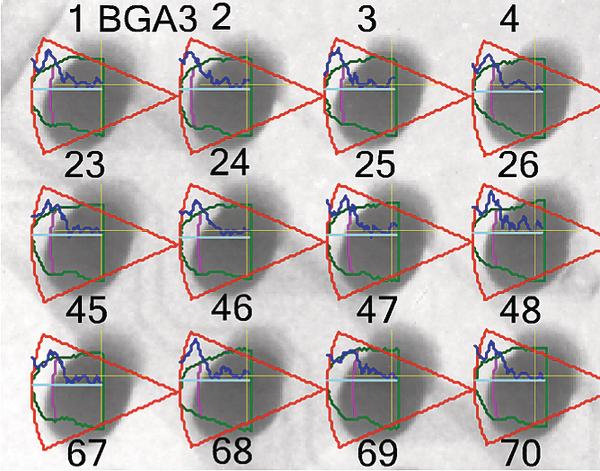
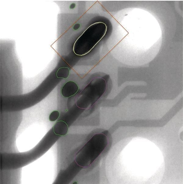
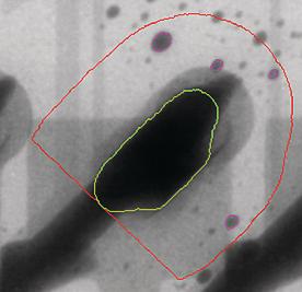
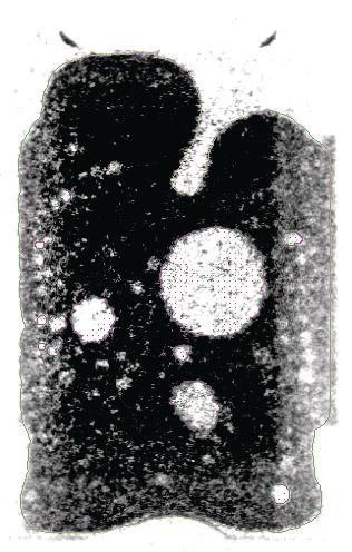
When manufacturing through-hole components, the connecting wires of leaded components are put through holes (vias) in the boards, the solder connection is formed at the bottom of the board either by the Selective Soldering process or Pin-in-Paste Method.
For a reliable performance, both the filling degree (Barrel Fill) within the via and the wetting on the soldering side are crucial. IPC-A-160 standard requires a minimum filling degree of 75%. By means of oblique views, the filling degree and stage of the solder menisci become visible. To this end, initially a reference area is defined based on a good pin and for further evaluation is divided in „barrel, land and destination solder“. From now on, the software will compare all pins with the specified reference pin and by subtracting, the percentage filling degree is determined. In addition, accidental bumps and shorts (bridges) in the immediate vicinity of the pin are made visible.
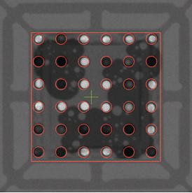
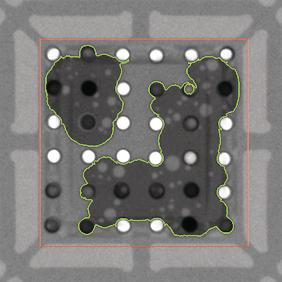
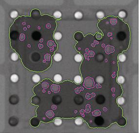
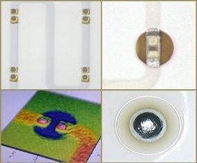
Void inspection in QFN packages
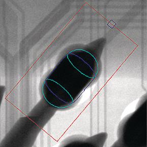
When manufacturing integrated power electronics, so-called „dies“ are often mounted directly onto a base substrate. In order to derive power loss in form of heat, the base substrate is usually soldered to a large area heat sink. To avoid deterioration of heat dissipation, these connections must show the lowest possible amount of voiding.
Voids can be detected by X-ray inspection, proceeding as follows: First, the search region is defined and set as a reference area. In this step, vias can already be excluded from the analysis. Then, the wetted area (appears dark on the lighter plate) is separated. The bright spots in the wet, dark areas show voids. The software calculates the percentage of voids in relation to the wetted and non-wetted area.
In many cases, the thermally conductive material under the component impedes the detection of voids. The component shown below sits directly on a 4mm thick copper layer. In addition to the inhomogenities produced by the copper and increase of the noise behavior, a significant reduction of contrast between solder and void is observed. To increase contrast and homogeneity, the images of plate and soldered component are separated using MatriX SFT (Slice Filter Technology).
These examples are just a selection from the range of current applications, which can be operated using modern X-ray inspection techniques and equipment. In addition to the appropriate inspection strategy, other important variables are crucial when selecting an X-ray inspection system, among others: layout of the manufacturing process, design and complexity of the manufactured products, production volume, required test coverage (is a 100% inspection of all products necessary?), inspection time and cost. Additionally, in modern production environments, the integration of inspection systems into the manufacturing environment is essential.
Zusammenfassung
Durch den Einsatz moderner Röntgensysteme werden nicht nur hohe Qualitätsstandards von Produkten sichergestellt, sondern mittels Echtzeit-Prozesskontrolle wird auch der komplette Produktionsprozess überwacht und optimiert. Gerade in der großvolumigen Fertigung spielt die Automatische Röntgeninspektion eine wichtige Rolle. Hauptanwendungsgebiet in der Elektronikindustrie ist die Inspektion von Lötstellen. Aufgezeigt wird der Einsatz industrieller Röntgentechnologie anhand aktueller Anwendungsbeispiele.
De par l’utilisation de systèmes modernes de radiographie, ce ne sont pas uniquement des hauts standards de qualité des produits qui sont assurés, mais au travers d’un contrôle de processus en temps réel, il est également possible de surveiller et d’optimiser le processus complet de production. C’est justement dans la fabrication des gros volumes que le contrôle automatique par radiographie joue un rôle. Le domaine principal d’application dans l’industrie électronique est le contrôle des points de soudure. Ce qui est mis en évidence, c’est la mise en œuvre de la technologie industrielle de radiographie au vu des exemples actuels d’utilisation.
Share:


