

The challenge when using miniLEDs lies in the processes of assembly and soldering of these tiny components onto PCBs, which accommodates the electronic circuit required for driving them. MiniLEDs have an edge length of 240 µm; solder pads that are required for the electrical connection are even smaller. In further feasibility trials, the printing of solder paste deposits smaller than 45 µm x 45 µm could be also achieved. The paste depot required for the assembly of the miniLEDs is specified by the size of the opening (aperture) in the stencil.
In order to apply the small solder paste deposits reliably, the paste needs to have solder powder particles that are smaller than 15 µm in diameter; similarly, the stencils must be manufactured with high precision. Paste application in this area with minimized geometries can only succeed if the printing system features high-precision alignment and if a special print head with optimum release behavior is used for the finest structures. Also, a measurement system that can reliably detect small geometries is necessary for high process reliability and control.
Further development and testing
With its expertise, the Application Center of the Christian Koenen company contributes to the development of both board assemblies and manufacturing processes in electronics. It serves as a collaborative platform so that the best possible solutions for demanding requirements can be developed with the customer. This center is air-conditioned and classified as a clean room in accordance with the high requirements for such an installation. These are fundamental prerequisites for ensuring that process conditions can be maintained at a constant level, as was the case in the following described test series.
In this series of experiments, each variant was printed 10 times on the PCBs without using solder resist. The stencil featured about 1000 apertures so that a statistically significant analysis was reliably possible. The bottom side was never cleaned during the printing process in order to reduce influencing factors and thus improve the comparison of the data. The prints were checked directly in the Meister S inspection system. To verify the results in the series of experiments, different microscopes and a Cyber laser scanner were also used. The printed circuit boards were then neither assembled nor soldered.
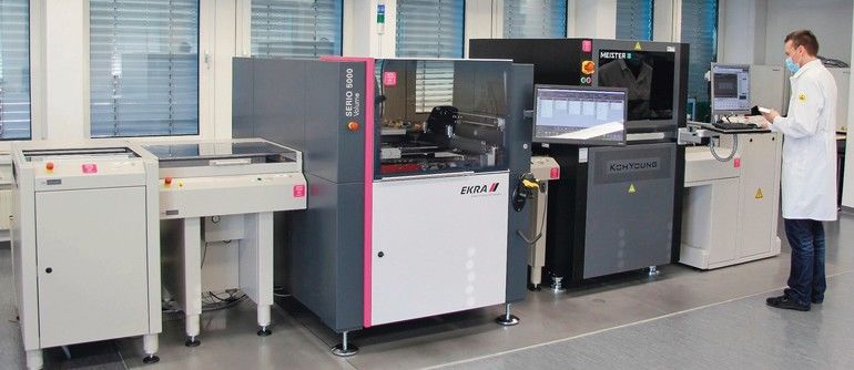
A reliable experimental setup was jointly realized with the partnership of Heraeus, Koh Young, ASYS, and Christian Koenen. The tests were carried out under real-world conditions, and commercially available components and materials were used.
Systems and materials used for the series of experiments were:
- ASYS SMD line consisting of Ekra Serio 5000 printer together with various transport and handling modules
- MiniLED solder pastes Heraeus LED131 (type 6) and LED100 (type 7)
- CK Nanovate Nickel stencils with plasma treatment
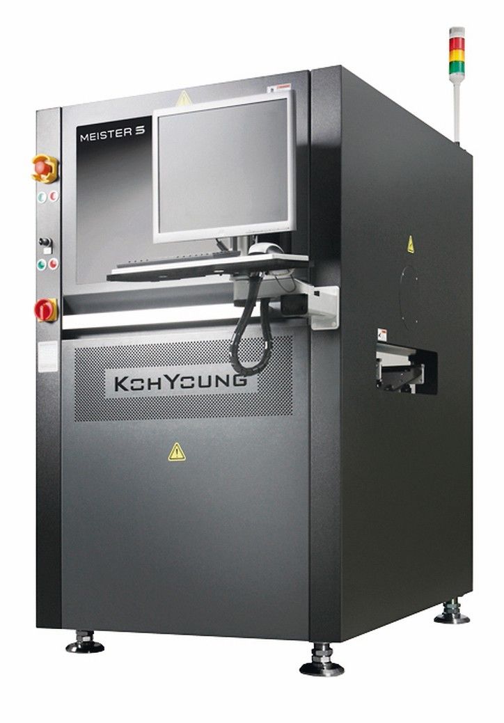
- Koh Young Meister S inspection system
Using the right solder paste
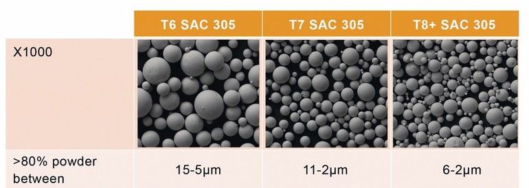
For the miniaturized miniLED pad geometries, ultra-fine solder powders with grain sizes of 15 µm are required to obtain reliable solder pastes to be used in this application. With stencil thicknesses between 15 and 30 µm and aperture openings smaller than 80 µm, these powders can reduce potential printing errors, such as fluctuating solder volumes or missing solder paste deposits. For the studies described here, solder powders of type 6/7 were used, produced by the patented Welco process. In this process, the solder alloy is heated in a thermally stable dispersion medium above its melting range. With the utilization of a special rotor-stator procedure, molten, homogeneous solder particles are produced. After cooling, the required solder powders were obtained with a narrow particle size distribution (type 6: 5–15 µm / type 7: 2–11 µm). They are characterized by sphericity (aspect ratio of ~1) and a smooth surface. These parameters help to guarantee good initial printability as well as in the long-term.
To ensure excellent printability as well as the necessary solderability, Heraeus has also developed a NC flux formulation series (LED131/LED100). Due to the smaller grain size, the surface area of the solder powder spheres increases (higher oxidation), so a formulation for activation had to be designed. The aim was to achieve excellent wettability of all partners involved, a low void rate, as well as maintaining the necessary insulation values (Surface Isolation Resistance) of the remaining flux residues. The requirements for solder pastes, such as low solder ball forming, ensuring sufficient tackiness prior to reflow is needed. This guarantees that the dies with their minimized connection areas remain in place until the reflow process was performed.
Improved stencil material
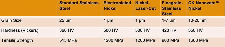
The CK Nanovate Nickel stencil material has been further improved by the Christian Koenen team in recent years, which resulted in the stencil material CK Nanovate Nickel. This super-alloy made it possible to cut nickel using a laser without the formation of micro-cracks. The material thus combines the advantages of stencils made of nickel and of stainless steel, but without their drawbacks. If the physical properties are compared, Nanovate Nickel yields significant advantages even with very thin material thicknesses.
Due to the small grain size of the material and its high strength, stencils with a thickness of 15 µm or more can be manufactured under standard serial production conditions.
For the formation of the small solder deposits of the miniLEDs as well as for the verification of the limits of printability, stencils with material thicknesses of 15 to 30 µm for the printing experiments were used. This allowed for the evaluation of different area ratios and filling degrees.
To ensure that representative results were obtained despite the selection of different sizes of mi niLEDs, the following aperture sizes were used: 45 µm x 45 µm; 60 µm x 60 µm; and 80 µm x 80 µm.
A further improvement in the printability of the small apertures resulted from the Plasma 3.0 coating of the underside of the stencil as well as of the inner walls of the apertures. The plasma 3.0 coating reduces the adhesion between paste and stencil, which results in a better release from the apertures and reduced volume dispersion between the individual depots and also between the subsequent printing cycles.
After optimizing the stencil layout and by using the optimal stencil technology (a frame-mounted CK Nanovate Nickel stencil with Plasma 3.0 coating), the paste deposits on the pads of the miniLED were printed with high reproducibility.
Modern paste printing
Modern paste printing systems are characterized by their high flexibility: EKRA printers can dynamically respond to changing requirement profiles. With the trend towards miniaturization, the necessity arises to achieve a reproducible paste transfer in the micrometer range. This also applies to the application described for the processing of the miniLED. The Serio 5000 printer platform used is a system that meets all current and future process requirements.
The flatness of the substrate and its coplanarity to the stencil determines the success of paste transfer. These influence the release behavior during the separation process. MiniLED substrates are susceptible to bending. If such applications are to be expected in the high-mix/low-volume manufacturing environment, then the MultiClamp transport system can be used in conjunction with a vacuum print nest. With its over top and side clamping bars, it supports the substrate to its edge beyond the end of the print nest. The retractable clamp will then draw the substrate flat. The result is an even surface for paste application. If the products of the types described here are the only ones being handled in production lines, dedicated transport systems can be employed.
Reproducible high manufacturing quality also requires operating conditions that are reliable and repeatable. For the test series, this was ensured by the design of the printing table in the EKRA system. The system guarantees that the substrate is fed to the stencil within the micrometer. As a result, optimum sealing is achieved for each individual printing process. The separation process has been optimized in speed and travel to suit the release behavior of the paste by the system‘s high-resolution servo motor.
EKRA‘s advanced print head, which was specially engineered for ultra-fine-pitch applications, also made an improvement to the results: The pressure of the squeegee moves precisely within a narrow tolerance window. In addition, the stencil is not subjected to any pressure during the separation process, resulting in positive effects on coplanarity and the even distribution of forces during the paste release.
All relevant print parameters are transferred to the Koh Young KPO inspection solution via the EKRA advanced closed loop interface, recorded, and automatically optimized. In that way, the squeegee and separation behavior can be fine-tuned for applications such as the highly miniaturized miniLED, without any intervention by the operator staff.
Inspection measurement evaluation
When using automated optical inspection, it is necessary to find a feasible compromise between inspection speed and measurement accuracy. This is important since a camera can only resolve a certain number of pixels. Pixel size, in turn, correlates with accuracy. The smaller, the more precise.
Processing miniLEDs in a SPI system is also about pixel size, meaning the smaller the LED, the better the resolution is on the display. For solder paste printing and inspection, this implies that small structures and low print heights must first be printed with high repeatability and then likewise inspected. For a repeatable measurement, the information of about 100 pixels is needed. This means that one can extrapolate from the pattern size to the required resolution of the inspection system. Another important aspect is the z-resolution. Optical measurement systems evaluate the gray-value phase shift between the single pixels. For this purpose, light is projected at a defined angle from the sides into the camera field. This means the projection angle and the pixel size correlate with the z-height resolution.
The design of the Meister S inspection system is tailored precisely to these requirements. Not only was the pixel size reduced here to 5 µm, but the projection angle was also minimized. Although this results in a reduction of the height measurement range by a factor of half compared to a standard SPI, high precision at low height is required in the specific applications for the Meister S system. In addition, the Plus version of the Meister machines is particularly optimized for reflective surfaces.
This investigation results underpin the system engineering approach and reveal the physical limits of optical inspection. The smallest aperture size of 45 µm does not meet the criterion of 100 pixels for the image. Therefore, a higher volume distribution of the measurement system was seen. Koh Young is already designing camera systems with a finer resolution of 3 µm. At the time of this test series, however, these cameras were not yet available. Such a system would reliably inspect aperture sizes 30 µm.
Successful miniLEDs test series
During these series of tests, reliably reproducible solder deposits could be printed with the paste formulations LED131 and LED100. With the stencil openings 80 µm and 60 µm, the best results were achieved on the EKRA Serio 5000 and inspected in line with the Koh Young Meister S.
By using a Heraeus solder paste type 8+ (2–6 µm powder size) in combination with a 15 µm thick stencil CK Nanovate Nickel featuring Plasma 3.0 coating, in further feasibility trials, the printing of solder paste deposits smaller than 45 µm x 45 µm could be also achieved.
For small depots and low stencil thicknesses, the sealing and release of the paste in the printing process are important for manufacturing success. Printing systems must therefore be able to provide outstanding solutions for maximum coplanarity between substrate and stencil. The squeegee printing, as well as the separation process, must be repeatable and finely tunable. In a nutshell: the continuous advancement of SMT manufacturing will thus continue.
HighTech Stencils
Otto-Hahn-Strasse 24
85521 Ottobrunn-Riemerling, Germany
Tel.: +49 89 66 56 18 – 0
E-Mail: info@ck.de
Website: www.christian-koenen.de
Durch Versuchsreihen für anspruchsvollen Pastendruck mit feinsten Strukturen wird bei der Verarbeitung von miniLEDs als Hintergrundbeleuchtung für LCD-Panels in partnerschaftlicher Kooperation der Fertigungserfolg sicher gestellt.
Grâce à des séries d’essais pour une impression à la pâte ardue avec des structures très fines, la réussite est garantie lors de la réalisation de miniLEDs assurant le rétroéclairage des écrans LCD dans le cadre d’un partenariat commercial.
Благодаря серии испытаний процессов для весьма требовательной печати паяльной пастой, позволяющей формировать тончайшую структуру, эта технология в рамках совместного сотрудничества успешно применяется при обработке мини-светодиодов, используемых в качестве подсветки для ЖК-панелей.


