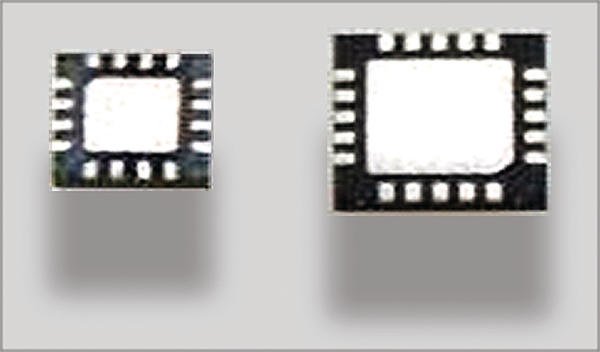
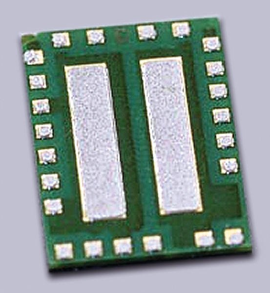
Flat no-leads packages such as QFN (quad-flat no-leads) and DFN (dual-flat no-leads) are becoming more popular in new component releases. Their very small form factor allows smaller packages, better grounding, and better heat sink thermal properties compared to other SMT packages.
William E. Coleman Ph.D., Photo Stencil, Colorado Springs (USA)
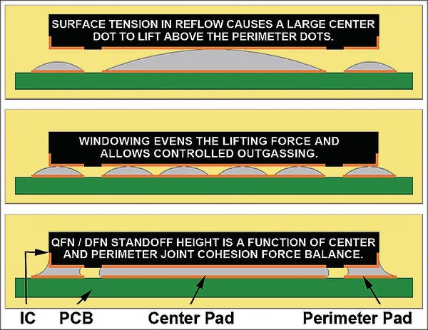
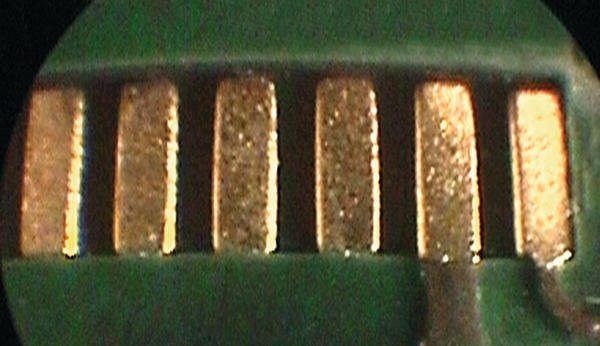
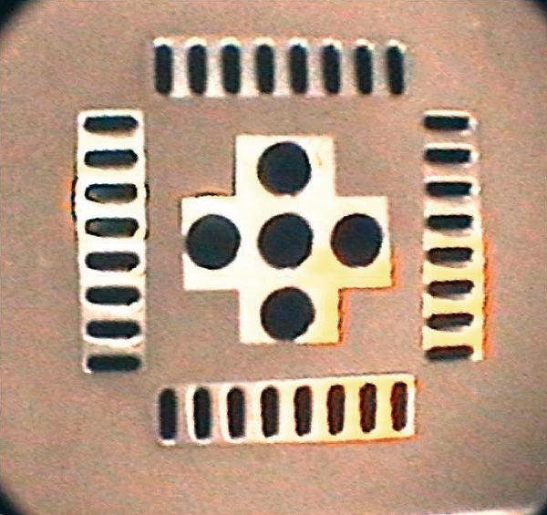
Most QFNs have a metal pad on the underside of the part for grounding and heat conduction. DFNs have a similar center metal pad but have leads on only two sides. Typical thickness of the QFN devices is .85mm and the body range from 3mm up to 12mm, so the packages are very small and very light. The QFN leads and ground plane conductor are flat and in the same plane on the bottom of the package. Printing solder paste 1–1 with the ground plane can cause the QFN to float during reflow, thus miss-registering the leads on the QFN and the pads on the PCB. QFN float can be controlled by reducing the amount of solder paste printed on the ground plane. Typically a 50 to 60% reduction will solve the QFN float problem. However the aperture reduction must be done judicially. A window pane aperture is recommended for most cases. This allows the solder paste volatiles to easily escape during reflow without moving the QFN device.
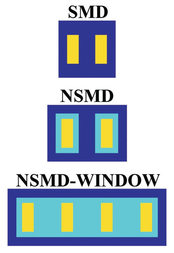
The next challenge is the actual aperture size in the stencil. Typical aperture widths as low as .175mm and aperture lengths as low as .4mm present a challenge to the printing process as far as percent paste transfer. The other challenge is the solder mask employed on the PCB. There are three types of solder mask designs: SMD where the pad opening on the board is defined by the solder mask, NSMD where the pad itself defines the boundary of the pad and the solder mask is pulled back off the pad (typically .05 to .075mm per side), and NSMD-window. In the last case there is no solder mask between pads so bridging between pads is more likely than with solder mask between pads.
Stencil and PCB design considerations
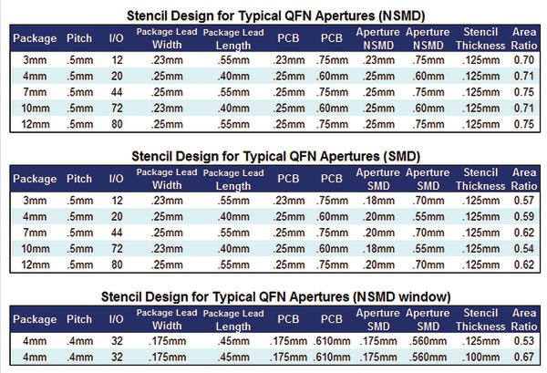
It should be noted that the recommended length of the pad on the PCB compared to the length of the lead on the QFN is .2mm larger. As seen the area ratio for a .125mm thick stencil is >.66 for all the examples listed. Aperture size for the SMD is .05mm smaller than the PCB pad. There are typically two reasons for this reduction. If the stencil is slightly misaligned to the PCB, paste could be printed on the solder mask. Also there might be high stress points if solder contacts the mask. The reduction in aperture size has reduced the area ratio making paste transfer more difficult. For area ratios below .66 electroform stencils or nano-coated stencils are normally recommended. One example is the NSMD-window. The pitch is .4mm leaving little room to put solder mask between pads on the PCB. Aperture size is also small giving a challenging area ratio for .125mm thick stencils; therefore .100mm thick stencils are normally recommended to provide a more robust stencil printing process window.
Another problem arises when using a NSMD window when the solder mask is higher than the pad on the PCB. In this case the solder paste is extruded through the stencil since the stencil is not in contact with the PCB pads during printing. This extruded paste will make contact with the bottom side of the stencil causing potential bridging during successive prints since there is no solder mask between neighboring pads. Stencil wiping after every print may help reduce this problem.
One possible solution suggested by a customer1 is a PCB side step stencil. This is an electroform stencil which is .08mm thick everywhere except in the QFN area inside the solder mask where it is .01mm thick. In this case the mask opening was of the order of .125mm per side except on the ends of the pad rows where it was less. There are several limitations to this approach. Namely the spacing between the step and the solder mask is extremely small allowing for little miss-registration. Also the stencil is thinner for all other components except the QFNs which may yield insufficient paste. The first limitation could be addressed at the PCB design level by making the mask to pad clearance much larger; of the order of .25mm per side as well as leaving the ground plane without any solder mask surrounding.
Another possible solution is a single level stencil without step but with nano-coating on the aperture walls as well as on the bottom side (PCB side) of the stencil. Nano-coatings have a property called fluxophobicity. Quite simply it is the stencils ability to resist the spread of flux on its surface. It is measured in the form of the ‘flux contact angle’. This is the angle that the flux will form when a drop is placed on the surface of the stencil. Nano coating not only increases the paste ability to release form the apertures but also to resist spreading on the bottom side of the stencil when the paste is extruded into a cavity created by the NSMD-window. This property not only eliminates the need for frequent under board wiping but also reduces the occurrence for pad to pad bridging.
QFN repair
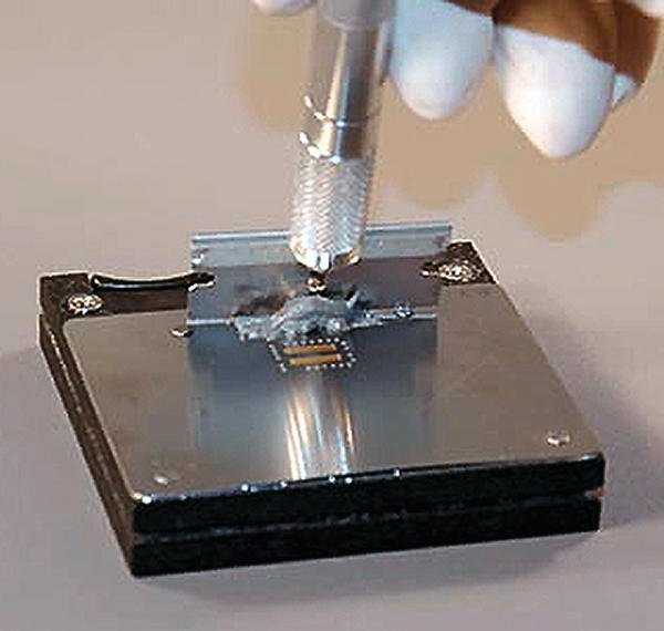
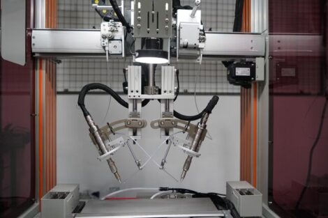
The first step to repair a defective QFN device is to remove the defective device from the PCB and clean the excess solder from the PCB pads. Solder paste is then printed either on the PCB or on the bottom of the QFN prior to placing the QFN on the PCB and locally heating to reflow the solder paste and solder the device in place. Mini stencils are normally used to print paste on the PCB. This can be a difficult and tedious task for very small QFN devices ranging in size from 3mm up to 12mm. Printing solder paste directly onto the QFN device is a more popular approach2.
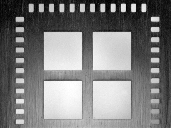
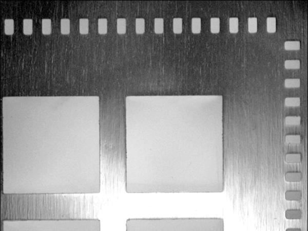
A possibility is a repair stencil that fits into a holding tool which also holds the QFN in registration to this stencil. The top portion of a 7mm / 48 I/O .5mm pitch repair stencil and the top portion of a 10 mm / 72 I/O .5mm pitch repair stencil are shown. Note that the aperture area for the ground plane is reduced by approximately 50% by the window pane technique. The paste printed on QFN pads using the tool that holds both the stencil and the QFN device. After paste is applied the QFN is placed on the PCB and locally reflowed.
Conclusion
Although QFN devices present a challenge to the SMT assembly process with proper stencil design, proper stencil technology selection (laser stencils, electroform stencils, nano-Coat stencils), and proper PCB solder mask layout these challenges can be overcome. The most popular QFN repair seems to be to print solder paste directly onto the QFN leads and ground plane.
References
- 1 Private communication with Greg Kloiber, Manufacturing Engineer Plexus Corp.
- 2 “BGA and QFN Repair Process” William E. Coleman, APEX 2008
Zusammenfassung
Das QFN- oder DFN-Package sind SMD-Bauteile, die keine Anschlussdrähte haben, sondern Anschlusskontakte auf der Package-Unterseite mit denen sie unmittelbar auf der Leiterplatte montiert werden. Der Artikel zeigt nun auf, wie die Herausforderungen beim Bestückprozess durch die richtige Wahl von Schablone und Lötstopplack überwunden werden können.
Le package QFN ou DFN sont des composants SMT sans fils mais dotés de contacts pour la connexion en dessous du package au moyen desquels ils peuvent être directement montés sur le circuit imprimé. L’article révèle comment les défis du processus d’équipement peuvent être relevés grâce à un choix judicieux des pochoirs et du masque de soudure.
Share:


