
Traditional methods of PCB production are not as cost effective or environmentally friendly as they could be as they use substantial amounts of power and produce unwanted by-products which need to be disposed of.
Chris O’Brien, Rainbow Technology Systems, Glasgow (Scotland/UK)
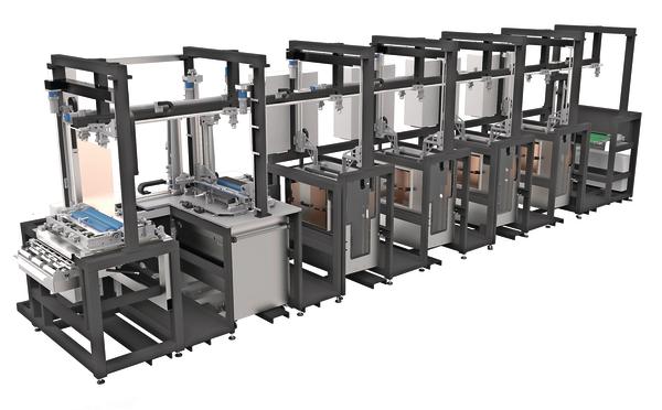
Six years ago Rainbow embarked on a journey to develop a PCB manufacturing system which was not only more effective but also better for the environment and more cost-effective to operate by substantially reducing the amount of utilities consumed in the process. The result of this research and development is the Rainbow Processing Unit which incorporates coating, imaging and development of PCB panels in one compact unit. Unlike traditional production methods, the Rainbow unit joins together several steps of the PCB manufacturing process into one fully automatic system, takes up under20sq m of floor space and comes complete with its own environmentally controlled enclosurewhich helps to maximize potential yields.
Solvent free
The process uses a solvent free liquid etch resist and lithographic film (standard photo tools) in the imaging process and is capable of producing up to 180 double-sided panels per hour. This high throughput even at fine detail levels is beyond the most up to date laser direct imaging systems. Energy saving is central to the process. There are no drying ovens that are typically needed for wet resist (which can consume 20kW to 70kW), no laminators that are required for dry film (averaging 20kW) and no light sources required for the imaging process beyond UV LED’s(saving typically 15kW). Overall the power consumption of the Rainbow unit for coating, imaging, developing, rinsing and drying is less than 9kW. One of the key advantages of the system is its ability to print fine line detail producing tracks under 20 microns. As the industry drives towards increasingly finer levels of detail, the Rainbow process is already capable.
Landfill
The company’s unique solvent-free resist is the key to the process and is also good for the environment. The coating is only 5-microns thick and is exposed in its wet state (no need for pre-drying). It is developed using industry standard chemicals (potassium carbonate or sodium carbonate). The use of wet resist has considerable benefits over conventional dry film. Firstly, the adherence of the resist to the copper is much improved as the process squeezes the resist into all the contours of the substrate – this closeness cannot be achieved with dry film as its semi-solid state tends to lead to bridging across peaks in the copper, which can lead to failures particularly when producing fine detail. Secondly, line growth is very small allowing finer detail to be produced as the optical path is shorter at 8 microns (only 5 microns of resist and 3 microns of phototool protection for the light to pass through) compared to typically 40 to 50 microns for dry film with its Mylar protection. This Mylar coating creates its own environmental problems as once the Mylar layer is stripped from the substrate it has to be disposed of in landfill. Mylar is not required for the Rainbow process. The low volume of resist obviously leads to lower buildup of waste in the process, reducing costs substantially.
High yields
The LED’s used for curing the resist are not particularly collimated at 6.5 degrees half angle, this brings advantage as any small particles that would typically cause shorts when using very collimated light will not prevent resist cure, improving yield. In addition as there are only a few seconds between the coating and imaging stages and the operation is carried out vertically with automatic transfer in a controlled environment, there are minimal opportunities for debris to attach itself to the wet ink. This contrasts with traditional production lines where the coating and curing processes are separated, and some manual handling may be involved.
Standard Phototools
Standard silver halide phototools are used in the process after being given a special protective coating using the company’s Panda Coater. This coating protects the phototool from moisture and chemical attack and allows release from the etch resist, which is brought into direct contact. Phototools are aligned and punched offline then loaded into a cart, which can quickly be exchanged ensuring fast turnaround between part numbers.
As well as the other savings already touched on from reduced waste, lower energy requirements and higher yields, the amount of water used in the process of the company in comparison to alternative processes is vastly reduced, improving the environmental impact of the process and offering further reduced costs. The accumulation of these various savings ensures a fast return on investment in addition to the enhanced capability.
Other opportunities
Aside from the PCB inner layer production that the Rainbow Process Line of the company has been developed for, the process is now being adapted for touchscreen applications with very fine tracks being printed double sided on clear substrates. Other development work around flexible materials is also being carried out, both for reel to reel and sheet based applications. In conclusion, the process of the company can not only make PCB manufacture more streamlined, faster and more profitable but promises to offer considerable savings in the cost of utilities alone, whist simultaneously reducing environmental impact and improving capability.
SMT Hybrid Packaging
Booth 9-320
Zusammenfassung
Traditionelle Methoden der Leiterplattenproduktion könnten kosteneffektiver und umweltfreundlicher sein, als sie es tatsächlich sind. Denn sie benötigen riesige Mengen von Energie und produzieren unerwünschte Nebenprodukte, welche entsorgt werden müssen. Abhilfe schafft nun ein neuer Prozess der Leiterplattenherstellung, der neben geringerem Energieverbrauch und Abfall auch höhere Erträge verspricht.
Les méthodes traditionnelles de production des circuits imprimés peuvent être plus avantageuses dans les coûts et plus compatibles avec l’environnement qu’elles ne le sont effectivement. En effet, elles nécessitent des quantités énormes d’énergie et produisent des résidus annexes indésirables qu’il faut évacuer et recycler. Actuellement un nouveau processus apporte une aide à la fabrication des circuits imprimés et il promet des revenus plus importants parallèlement à une consommation d’énergie plus réduite et à moins de déchets.
Share:


