
Semiconductor probe pins are approaching a crunch point. Silicon geometries are getting ever finer, and packaging density has been increasing for SMT ICs, LCDs, fine-pitch glass substrates, and other electronic components. Such high-density devices require inspection in many areas, so multiple probe pins must be placed with a very small spacing between each. The package unit pitch for recent devices is only 0.4 to 0.5 mm. In a few years, it is expected to be 0.3 mm or less. Yet the probes used to connect to and test these devices are manufactured with the same stamping and pressing techniques as they have been for many years.
A new electroforming (EFC) technology is emerging which overcomes many of the limitations of stamping and pressing. EFC enables the creation of probe pins that are not only much smaller, but also lower resistance and higher performance. EFC probe pins can not only support much narrower pitches, but also offer benefits for testing at high frequencies, very low voltages and high currents. This paper describes electroforming (EFC) technology and looks at the contribution that it can make to semiconductor manufacturing and testing.
What is electroforming?
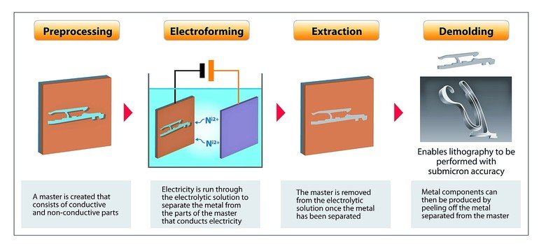
Electroforming is a metal forming process that forms ultra-thin metal components through the electroplating process. The components are produced by developing a layer of metal onto a base form (master). Once the plated layer has been built up to the desired thickness, the newly formed part is stripped off the master substrate.
Microfabrication technology allows for considerable component design flexibility and is also used to meet more exacting needs for shapes and sizes, since it enables the transfer of a pattern with submicron‐scale (0.0001 mm) surface roughness accuracy. Unlike electroplating, electroforming builds thicker, stronger metal layers which become the actual contact structure and enables high-precision production of extremely small, thin and fine patterned parts.
Benefits of EFC
Omron has introduced electroforming technology into the fabrication of the semiconductor probe pins, which were previously formed with presswork. This enabled forming narrow parts with a high aspect ratio (ratio of thickness and width). Plates with a width one-third of their thickness have been produced. With traditional pressed contacts it is difficult to allow the plate width to be less than the plate thickness.
With electroforming, it is also possible to bend contacts much further. Traditionally, a plate can be bent to a radius of up to twice the plate thickness by dynamic mechanical tooling. Electroforming has achieved a 0.04 mm bend radius by transferring pattern with static chemical processing. This allows for much more freedom in creating round shapes, opening new possibilities in component design. EFC has also allowed micro slits of 35 microns and holes of 50 microns to be created. These were not possible with traditional presswork.
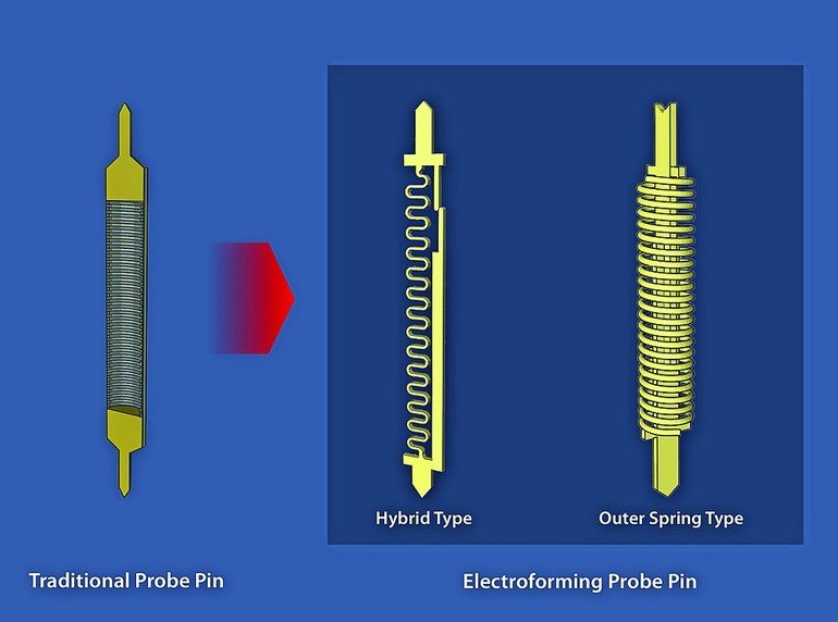
Using EFC an entirely new style of pin has been created, combining four components (upper and lower plungers, spring and conductive path) into one. They have a flat structure which enables placement of pins at any angle, thus making it easier to reduce pitch compared to a conventional cylindrical probe pin. The versatility of electroforming technology enables a single component to incorporate a spring section to provide contact force and durability, and a barrel section that turns on power when it fits the plunger, separate from each other. No electricity flows through the miniaturised spring section, thus solving such problems as excessive temperature rise, the spring section‘s disconnection, and unstable resistance. Since there is no need for costly investment in press dies and other equipment, as well as the time-consuming die-making process for prototyping and mass production of probe pins, specific demands for customised non-standard specifications can be satisfied speedily.
Omron has produced flat probes of 60 microns thickness, and sockets of 150 micron pitch can be assembled. EFC probes can also be very robust. The larger 0.6 mm diameter outer spring type can handle up to 2 A. To assemble these tiny contacts, a special air tweezer tool has been created.
Addressing the issues
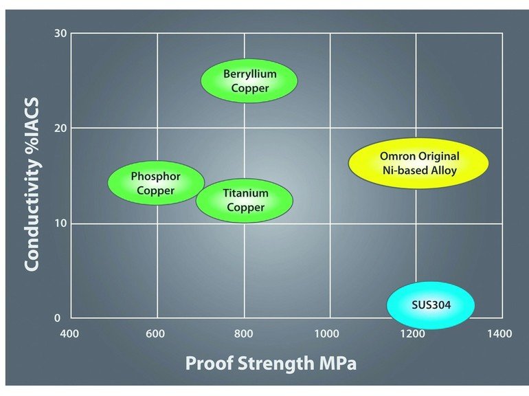
One of the most fundamental benefits of electroforming is that harder materials can be used – leading to greater resilience. In order to reduce the damage to components when attempting to miniaturise them through press work, softer Copper alloys with lower strength have been used, leading to greater deformation under pressure during tests. Electroforming allows complex shapes to be manufactured in harder, Nickel alloys reducing deformation under pressure as well as the risk of breakage.
Another issue is contact failure due to contamination on the pad of the device under test (DUT). Since electroforming allows complex shapes to be manufactured, a number of solutions are available here. A ‘wiping’ structure can be created at the end of the probe pin to remove contamination for example. Alternatively, probe pins with multiple plungers can be designed which maintain reliable contact even if one plunger is blocked by contamination.
Kelvin sensing, requiring four probe pins, is a particular challenge with traditional, larger probes. However, electroforming techniques allow the creation of a compact, monolithic Kelvin sensing probe pin.
Power devices present their own unique test issues. A critical problem is heat generation due to contact bias. Using electroforming techniques, a bundle of probe pins can be created which can all maintain contact even where bias is present. Such bundles can deliver as much as 30 A in a 1 mm area.
A further issue is the inductance of the pins that can have a negative effect on rise time. The improved characteristics of electroformed materials and their greater hardness means that the length of the coil spring can be reduced to reduce inductance. If required, a plate spring can be created to ensure minimal inductance.
The smoothness of electroformed contacts is an advantage when testing very high frequency semiconductors of 100 GHz or above. High frequency currents tend to travel on the surface of the conductor (skin effect) and roughness of the surface extends the current path and hence the losses. With EFC technology, burs on cut edges and warping (undercutting) that are unavoidable with presswork do not occur. A roughness average (Ra) of less than 0.1 micron can be achieved with EFC, compared to typically 2 microns with pressed contacts.
The future
After many years stagnation, EFC looks like the advance semiconductor test engineers have been waiting for. Semiconductors are not only getting more compact, but higher frequency, higher power and lower voltage devices are emerging too. The improved performance of EFC supports offers benefits for all of these devices and enables the manufacture of more durable probes too.
http://components.omron.eu/
Share:


