
Zero defects means never delivering a defective product to a customer. Manufacturers of Printed Circuit Boards (PCBs) are doing absolutely everything in their power to make this happen – knowing full well that they cannot possibly achieve this 100 %. JTAG Technologies of Eindhoven has developed a test device that further reduces the risk of slip (i.e. defective PCBs being sent to a customer). Tbp electronics, a manufacturer of PCB assemblies in Dirksland, contributed to this development.
Peter van den Eijnden, Managing Director, JTAG Technologies
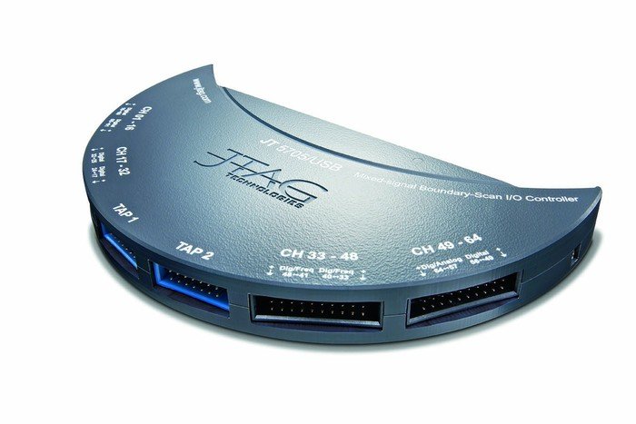
The new controller, which recently became available, tests PCBs for structural (assembly) defects, i.e. not functional (design) defects. This is done using the tried-and-tested ‘boundary scan’ method, the greatest advantage of which is that you cannot only immediately see that the PCB is defective, but also where the defect lies. What is new is that the test device not only measures digital but also analogue signals – thereby enabling PCB manufacturers to take the next step towards virtually error-free assembly.
3,500 error probability
Peter van den Eijnden, Managing Director and owner of JTAG Technologies, calculates that the average PCB easily contains around 500 components and a total of around 2,500 soldered joints.
“With this kind of printed circuit board, you run the risk of 3,500 errors. And, with a larger PCB, the error probability can easily be around 10,000 – while a single error can result in a defective board.”
These are structural errors, such as the wrong components (resistance values, capacitors, etc.), incorrect polarity, lacking components and incorrect or lacking soldered joints.
PCB manufacturers like tbp electronics are working hard to prevent this. Firstly, they only work with the best component suppliers (“We’re talking component errors in the order of magnitude of parts per million,” says Van den Eijnden) and continuously investing heavily in state-of-the-art assembly machinery (“Automation reduces error probability”) and, secondly, they lead the client’s engineers in the direction of Design for Manufacturing (DfM), so that they design the PCB in such a way that it can be assembled with the lowest possible chance of defects. A step further is Design for Testing (DfT), in which the ‘easily testable’ aspect is incorporated into the design process.
Systematic testing
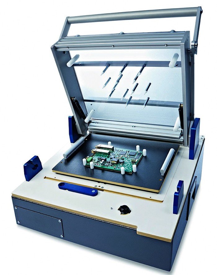
“There are all kinds of rules for DfM and DfT,” says Van den Eijnden. “If you stick to them, you’ll increase the quality of the assembly: your first-pass yield will be higher and, consequently, the risk of introducing errors smaller. But zero errors and 100 % perfect PCBs? That’s impossible. It’ll never happen.” But you can get closer. And there’s also progress to be made in preventing defective PCBs from being sent to the customer (‘slip’). “If the customer places a board in his product and it doesn’t work, well, that’s going to cost a lot of time and money.” This can be prevented by testing every board at the end of the production flow – systematically. “That’s the crux: you want to be able to test for assembly and production errors, especially the strength of the soldered joints, using a method that is inexpensive, guarantees the highest possible level of error detection and, if an error is detected, immediately shows where in the board it’s located.” The methodology devised in the mid-80s to do that is called the ‘boundary scan’. It was developed by Philips Research and then further refined by a company cluster to become the international JTAG standard IEEE Std. 1149.1 (1990).
Next steps
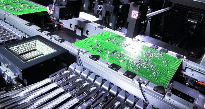
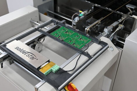
Systematic testing was already done before using ‘beds of nails’. Van den Eijnden explains, “Systematic testing was made possible by physically connecting the bed of nails, to which the measurement equipment was connected, to a PCB. This was not only expensive, but also no longer sufficient for the new PCB technology that was becoming more commonplace at the time, namely Service Mounted Devices (SMD). In order to take the next steps in the miniaturisation of the electronics, more – and smaller – components were needed on the circuit board. This was only possible by no longer pricking into the board, but by soldering onto it. That’s SMD technology.
The JTAG/boundary scan makes it possible to test SMD boards satisfactorily and inexpensively, he explains. In a nutshell: ICs with a boundary scan have a serial interface that is dedicated for test data. That interface lets you access every pin on the IC – and ‘direct’ and measure it. This also makes it suitable for component programming and software debugging. “As a matter of fact, most PCB developers are familiar with the JTAG/boundary scan because of this. That you can use the same interface for testing is something a lot of people don’t know. This is due in part to the fact that testing is not taught anywhere; you learn it in the business world.”
Global added value
How does the test method work? You have a PCB with chips on it with a serial data input and output. This lets you access all pins on the board and, consequently, determine whether the soldering is good. Insert a signal into the one end and see whether it comes out the other end. If not, something is wrong. The testing process can then be fine-tuned so that it is possible to determine very precisely which area of the PCB contains the defect. The equipment from JTAG Technologies, which originated in 1993 from a buy-out from Philips, automates the test process. “Our products make detecting and locating errors easier and more efficient. This reduces the need for expensive employees who spend a day or so figuring out where the error is on a board.” The global added value for customers is apparent, as this test equipment has placed this Eindhoven company at the forefront at an international level. “More than 95 % of our sales are from outside the Netherlands,” says Van den Eijnden.
Breaching the analogue ban
Its broad and diverse clientele enables the company to continue investing in innovations. The new controller, the first and, for the time being, only one that can handle both digital and analogue signals, is a good example of this. Van den Eijnden says, “An analogue standard is available, but not used. That’s no help.” His company believes it can breach the analogue ban with its Mixed Signal Boundary i/o Control, which uses a clever method – the tried-and-tested JTAG/boundary scan method – to make the phase between the digital heart of a microprocessor and analogue outside world testable. Partner-in-crime tbp electronics, which is continuously looking for ways to prevent slip, already uses it. Now other PCB manufacturers can buy it, too.
productronica, booth A1-458
“Our products make detecting and locating errors easier and more efficient.“
Peter van den Eijnden
Share:


