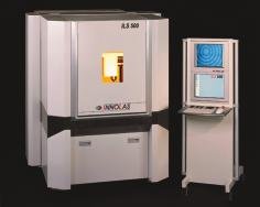
The InnoLas ILS500 laser system can be used for PCB and ceramic substrate prototyping and small production series. The equipment has been adjusted so that typical processing steps in the manufacture of circuit boards are reliably be carried out in a single operating cycle. These steps include, for example, laser drilling of micro vias (40 to 250µm diameter), direct structuring of metallic and organic layers, creation of ultra-fine conductor structures starting from 15µm (also structuring of copper) and cutting of flexible, rigid-flexible and thin multilayers. The ILS500P is equipped with a UV solid-state 7W laser, wavelength 355 nm, and a pulse repetition frequency of up to 100kHz. There is the option of integrating a second laser so that PCBs made of other materials can be processed effectively in the same system: this cane be ceramic Al2O3 substrates by means of a CO2 laser. The motion system mechanism is mainly a combination of a XY-table and a galvo-scanner. The scanner supports highly dynamic movements in the processing field with a size of up to 50x50mm, whereas the axes of the XY-table enable quick stepwise motion from field to field or coverage of the distances over large structures. Operation is supported by post-processor software for generating machine programs from CAD data in a great variety of formats (Gerber, Excellon, GDSII, HPGL, DXF, DWG).
EPP EUROPE 429
Share:


