For the non-destructive quality control and failure analysis of copper-filled microvias and similar interconnections, such as TSV, 2D X-ray inspection with nanofocus tubes and highly resolving detectors is a very useful tool. Latest highly resolving computed tomography (nanoCT) enables even the inspection of complex 3D integrated electronic devices and packages by 3D-visualisation and slice by slice analysis on the sub-micron scale.
Holger Roth and Tobias Neubrand, GE Sensing & Inspection Technologies, Wunstorf (Germany)
In this article inspection results for the 50–60 µm microvias of an defective embedded chip package are shown. The microvias were inspected non-destructively by both highly resolving microfocus computed tomography and improved digital X-ray imaging. Voids were found within the via fills and open interconnections between vias and pads were detected by the X-ray inspections. These defects could be verified and visualised in three dimensions by nanofocus CT.
Further, Trough Silicon Vias (TSV, about 100 µm in diameter) as used in 3D integrated electronic packages were inspected non-destructively by highly resolving nanofocus computed tomography (nanoCT). In particular, voids in the TSVs plating were visualised and quantitatively evaluated by numerical processing of the resulting volumetric data. The nanoCT technology is outlined and further applications such as interposers etc. are considered.
IC Minaturisation drives 2D and 3D inspection
Microfocus X-ray inspection of classical package features such bond wires, die bonds, mouldings and seals is a proven tool for spot checks and production control. Package miniaturisation lead to higher density and smaller size of internal structures such as microvias and FlipChip interconnections, demanding for resolution in the sub-micron range at extremely high magnification as provided by nanofocus tube technology.
From the resulting miniaturised and highly integrated devices new challenges arise for non-destructive inspection. For X-ray technology we may state:
- the features become smaller and cause less contrast in the 2D X-ray image
- many structures may confusingly overlap and conceal each other in the 2D X-ray image
In other words, we are facing two main development needs:
- highly resolving inspection in three dimensions, that is nanofocus and microfocus computed tomography
- improved signal-to-noise ratio in (real-time) X-ray imaging.
The conventional 2D X-ray inspection of miniaturised devices frequently will be affected by confusingly overlapping structures, if they can be imaged at all. This is to say, 3D integrated devices or systems require non-destructive inspection slice by slice or in 3D visualisations as provided by computed tomography (CT). However, until recently, many laboratory CT systems are using X-ray tubes of some microns focal spot size and maximum tube voltages around 100 kV. Since electronic devices contain very fine structures and strongly absorbing materials like gold or copper this results in unsatisfying image resolution and strong image artifacts, respectively.
X-ray inspection and computed tomography
The 2D nanofocus images were carried out with a compact laboratory X-ray microscope and CT system (phoenix nanome|x 180, GE Measurement & Control Solutions) dedicated to the analysis of electronic packages at submicron resolution. The system comprises a 180 kV high power nanofocus X-ray tube with a focal spot size down to below 1 µm. To improve the signal-to-noise ratio in X-ray imaging, a novel temperature stabilized digital X-ray detector array (GE DXR,1 Mpixel, pixels size 200 µm x 200µm) with a maximum frame rate of 30 fps was utilised, partially in combination with diamond supported tungsten target for higher X-ray intensity. Additionally, the system is equipped with an image intensifier-camera chain (4 Mpixel). This dual detector combination allows high resolution CT and low noise live imaging with short exposure times on the one hand and extremely high magnification 2D analysis with the images chain on the other hand. The system provides a 3D maximum voxel size of <1 µm (800 nm) and a 2D detail detectability of up to 200 nm.
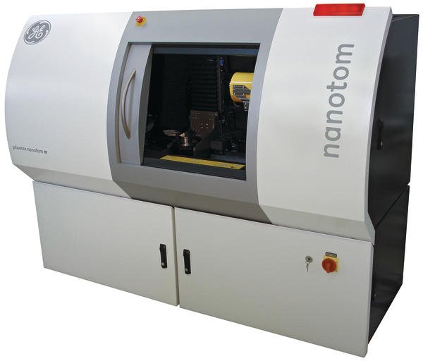
The 3D nanoCT scans were carried out with a recently released compact laboratory CT system (phoenix nanotom m 180, GE Measurement & Control Solutions, figure 1) dedicated to the analysis of small samples at micron voxel-size. The system uses a 180 kV/15 W high power nanofocus tube with a focal spot size below 1 micron and a 7.3-megapixel GE DXR flat panel detector with an active area of 307 mm x 240 mm (3072 x 2400 pixels, 100 µm pixel size) and a 2-position virtual detector (up to 4500 mm effective detector width), providing a voxel size of up to 0.3 microns. The influence of vibrations as well as thermal expansion and drift are minimised by a granite based manipulation system, vibration damping, low expansion materials and temperature stabilisation. Minor remaining drifts during long term measurements are monitored and compensated by the CT reconstruction software phoenix datos|x 2.0, which utilises efficient algorithms for geometry calibration, detector calibration, noise suppression, beam hardening reduction and region-of-interest-CT (ROI-CT).
A volume tomography system acquires a series of two-dimensional X-ray images while progressively rotating the sample step by step through a full 360° rotation at increments of less than 0.5° per step. These projections contain information on the position and density of absorbing object features within the sample. This accumulation of data is then used for the numerical reconstruction of the volumetric data.
Resolution of X-ray images and nanoCT
The geometric resolution V of an X-ray system, is given by the pixel size P divided by the geometric magnification M=FDD/FDO, i.e.: V = P/M. With a pixel size P=100 µm and a FDD = 600 mm a voxel size of <1 µm can be easily achieved at M >100. The final limitation of resolution yet is the focal spot size F of the X-ray tube, which causes an additional unsharpness of the image on the detector. Hence, for sub-micron computed tomography or X-ray inspection an X-ray tube with a focal spot size below 1 µm is required (nanofocus tube). In computed tomography a further geometric limitation to resolution arises from the overall size of the sample: to achieve an ideal image quality the sample should remain within the cone beam during the whole rotation. That is to say, the full sample diameter should be continuously imaged onto the detector, thus the magnification is limited. Nevertheless, due to improved reconstruction algorithms (ROI-CT), magnification and resolution may be increased further, inasmuch as some noise-like disturbance in the final 3D data can be accepted. For a very wide object like a printed circuit board assembly one may reduce even the rotation angle at the expense on the volume resolution in beam direction.
Inspection results for microvias
The sample first inspected is a QFN-A embedded chip package, manufactured by Fraunhofer IZM, Berlin, Germany. The excellent contrast resolution of the digital detector array can be seen from the glass fibres in the substrate displayed in the background. The vias turn out to be shifted against their Cu pads. The copper fill appears brighter in the centre, indicating voiding. The next samples are taken at high total magnification with the image intensifier image chain. While the image is noisier and less contrasted than at the DXR flat panel X-ray detail, the magnification is remarkably higher. Easily the central voids can be identified and it can be detected that the vias do not touch the pads.
In prior to the tomographic scans of through silicon vias as used in 3D integrated electronic packages, highly resolving 2D X-ray images for comparison and for orientation were taken. In oblique view at high magnification the vias and some internal void in the copper filling are plainly displayed, but some vias are concealed by the solder bumps. Adjacently the area shown at the digital nanofocus X-ray image was scanned by the described tomography system at voxel size of 1.25 µm at a magnification of 40 fold. With tomographic slice in the plane of the via axes there is shown that the internal voids in the via fill are plainly displayed. In the tomographic slices of another example an oblong void in the copper via filling is displayed and the voids may exactly be localised. Also measurements of, e.g., void and via diameters may be performed. At the tomographic voxel data after automatic void detection the three-dimensional shape of the vias and bumps is inspected by means of a virtual section. The voids cannot only be seen and inspected but also be automatically detected in order to statistically evaluate their size and volume.
Conclusions
2D X-ray inspection with nanofocus tubes and highly resolving detectors is useful for the non-destructive quality control and failure analysis of copper-filled microvias and similar interconnections, such as TSV. Novel flat panel detectors provide an image of superior signal-to-noise ratio in about the same averaging time a highly resolving image intensifier chain needs to reach its much poorer image quality.
However, the image intensifier still achieves a remarkably higher magnification and resolution. So, for the time being, still a combination of both detectors may be recommended for maximum versatility and increased image quality due to the low noise of the improved flat panel detector.
Also, for CT, the quality of the tomographic slices can be remarkably improved by the low noise and definition of the GE DXR detector images without increasing the scan time, as compared to previous detector systems. nanoCT, i.e., highly resolving computed tomography, enables the inspection of complex 3D integrated electronic devices and packages by 3D-visualisation and slice by slice analysis on the sub-micron scale. This novel tool in non-destructive 3D-microanalysis will – in combination with 2D nanofocus X-ray inspection – partially replace destructive methods, saving costs and time per sample inspected.
A typical application will be through silicon vias even at projected diameters of 20 to 30 µm as well as flip chips solder in 3D integrated devices. Digital Processing of the volumetric data enables dimensional measurements within the three-dimensional package structure.
ZUSAMMENFASSUNG
Bei komplexen Baugruppen, deren innere Strukturen sich im konventionellen zweidimensionalen Durchstrahlungsbild überlagern, liefert hochauflösende Computertomographie klare Aussagen. Sie eröffnet inzwischen eine Vielzahl von Analysemöglichkeiten, die mit herkömmlichen 2D-Röntgensystemen undenkbar sind – dank der nanofocus-Röhrentechnologie auch mit Auflösungen im Submikrometerbereich.
Pour les modules complexes dont les structures internes se superposent dans la radioscopie bidimensionnelle conventionnelle, la tomographie par ordinateur à haute résolution fournit des informations claires. Elle offre actuellement une multitude de possibilités d’analyses, impensables avec les systèmes radiologiques 2D courants – et grâce à la technologie des nanotubes, également avec des résolutions de l’ordre du nanomètre.
Acknowledgements
We thank Fraunhofer IZM, Berlin, Germany, for preparing the QFN-A embedded chip package. The TSV samples have been kindly provided by Applied Science & Technologies Research Institute (ASTRI), Hong Kong.
Share:


