
In today’s electronic design and manufacturing climate there is an increasing emphasis to improve product yield by improving quality and streamlining manufacturing processes in order to improve competitive advantage and lower costs. The ability to systematically verify that board designs have been developed with adequate DfT (design-for-test) in mind is crucial in determining a product’s overall testability and in defining the optimum test strategy for achieving maximum fault coverage. It also means that design and test people can work far more efficiently because all designs will be analysed in the same manner, using industry standard and company specific DfT guidelines.
TestWay’s electrical DfT analyzer enables design validation at the schematic capture stage, to ensure that adequate measures have been included to comply with the manufacturers test requirements. This is particularly important when adopting electrical test strategies such as In-Circuit and Boundary Scan, where adequate DfT must be correctly implemented at the earliest stage in the design cycle. Similarly test people can utilize TestWay’s test coverage analyzer to evaluate theoretical fault coverage aligned to various test strategies, to identify where fault coverage and testability improvements should be made. Resulting in increased cost savings and higher production yields by improving test efficiency in terms of fault coverage.
How it works
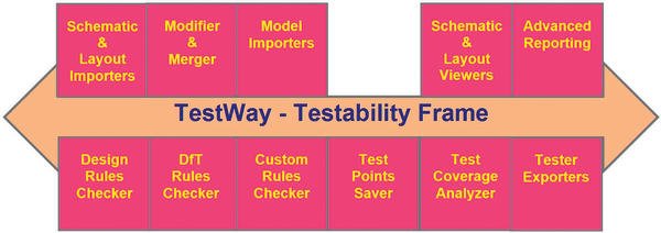
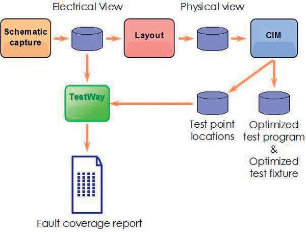
The TestWay open architecture is based on a testability framework that interfaces to a variety of plug-in modules, that provides both import and export opportunities, as shown in figure 1. In order to conduct an analysis, the board level netlist (schematic or layout) and component model libraries must be read. From this information, basic topological analysis, symbolic simulation and rule checking can be made, using topological data, accessibility data or both. The testability analysis results are reported in a natural language that can be used by design and test people to validate that specific DFT criteria has been implemented correctly.
Rules checking
Electrical rules’ checking is distributed into three main categories:
- Design rules
- Testability rules
- Boundary-scan rules
These rules are derived from formal standards and include rules commonly applied throughout the electronics industry. They are complementary to the DfM and test point placement rule checking features of commercial CIM systems. Specific customer requirements can be specified in a natural language using the custom rules feature. TestWay’s electrical rules checking can validate company specific DfT requirements in real time and are easily customized to reflect updates to testability guidelines.
Test coverage analysis
Test coverage calculations for PCB (printed circuit board) are becoming increasingly important as a key indicator in determining the quality of a product. In the majority of cases PCB structural test strategies that include test and inspection techniques such as in-circuit test (ICT), flying probe test (FPT), automated optical inspection (AOI), automated x-ray inspection (AXI) or boundary-scan test (BST), are perfectly adequate in detecting the majority of manufacturing structural faults. However, there are situations where the optimum test coverage is not achievable through structural testing, or it may be that the current test strategy provides inadequate structural test coverage due to limited access. Under these circumstances it may be beneficial to evaluate the test coverage contribution provided by functional test (FT) to detect structural defects.
The manufacturing process is not free from introducing faults due to the capabilities of the equipment and the process used. Typically, the defect universe comprises of the following categories:
• Missing devices
• Wrong value, 10 K instead of 100 K
• A dead device, e.g. ESD damaged or cracked device
• Mis-orientation rotated 180 degrees
• Device misalignment
• Tombstone effect
• Broken lead
• Short between adjacent pins caused by solder bridge, bent pins or mis-registration
• Open solder joint
• Poor solder joint, due to excessive, insufficient or malformed solder
Subsequently it is important to categorize these defects in relationship to a group of test coverage facets that provides a logical link with the production process. It allows the model to be clearly understood by designers, project management, test and production people. These test coverage facets are defined by three accepted de-facto standards for modelling test coverage, namely:
- MPS – Philips Research [1]
- PPVS – Aster Technologies [2]
- PCOLA/SOQ – Agilent Technologies [3]
The manufacturing flow comprises of three stages that determine
- The supply of correct materials
- The correct placement of components
- The soldering of components to the PCB
The correlation between the ‘defect universe’ defined by the various models and the different test coverage facets are shown in figure 2.
Test coverage evaluation
By reading the real test programs or coverage reports from the various test systems used within the manufacturing process, TestWay can control real test efficiency against theoretical. A ‘step-by-step’ analysis of application specific test programs, determines the measurement type and the defects that can be detected. This allows cost efficiency estimations to be made for a variety of test scenarios, to enable customers to select the correct test strategy for providing the optimum yield at the lowest cost.
Test point saving
With the dramatic increase in device density on PCB’s resulting in high net counts, it is virtually impossible to gain physical test access to each net for test purposes. In balancing different complementary test approaches, such as in-circuit test (ICT), flying probe test (FPT) and boundary scan test (BST), TestWay optimizes the total amount of locations where physical test access is mandatory. Furthermore the test point optimization data can be
- Integrated with CAD layout tools to identify where physical access is required
- Back-annotated into the schematic design
- Integrated with commercial CIM tools to identify where probes are required
In addition, physical confirmation is provided that the requisite numbers of test points are placed once layout is complete (figure 3).
Data reporting and visualisation
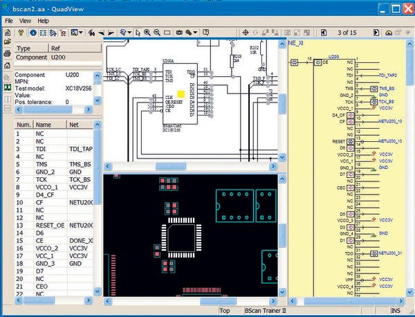
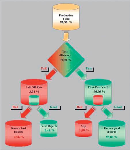
One of the problems in providing a comprehensive database of information relating to testability and fault coverage is the ability to present the relevant information in a manner that can be easily understood by the user. TestWay is integrated with a powerful and flexible viewer QuadView, which allows users to view testability violations and test coverage results in both the schematic and layout views. Fully customizable reports can be exported in a variety of formats such as Microsoft EXCEL, XML, HTML, Crystal reports, ASCII and graphical files. Reports can be used to show the theoretical production yield calculated from historical DPMO data, based on the defects that will be detected by a combination of test and inspection systems such as in-circuit, flying-probe, boundary-scan, AOI and X-ray, etc.
EPP Europe 548
zusammenfassung
Im Beitrag geht es um die Familie von Testabdeckungs-Werkzeugen, die auf dem Testcoverage-Tool der Referenzklasse TestWay beruht. Sie ermöglicht es Anwendern, die Berechnung und Analyse der Testabdeckung für eine Vielzahl industrieüblicher Tester durchzuführen. Derzeit werden über 20 Testermodelle aus den Bereichen AOI, AXI, BST, FPT, ICT und MDA unterstützt.
L’article se penche sur la gamme des outils de couverture de test basée sur le Testcoverage-Tool de la catégorie de référence TestWay. Elle permet aux utilisateurs de procéder au calcul et à l’analyse de la couverture de test pour un grand nombre de testeurs courants dans l’industrie. Actuellement, plus de 20 modèles de testeurs des domaines AOI, AXI, BST, FPT, ICT et MDA sont pris en charge.
L’articolo esamina la famiglia di strumenti per il test coverage basati sul test coverage tool della classe di riferimento TestWay. Gli utenti sono in grado di eseguire calcoli e analisi del test coverage di una serie di tester utilizzati in campo industriale. Attualmente sono supportati oltre 20 modelli di tester dei settori AOI, AXI, BST, FPT, ICT e MDA.
References
[1] Board Test Coverage – The value of prediction and how to compare numbers: Wouter Rijckaert, Frans de Jong; International Test Conference, 2003.
[2] Board Defect Coverage Analysis (From design to production): Christophe LOTZ; DATE 2004, Paris
[3] Test Coverage: What does it mean when a board test passes? Kathy Hird, Kenneth P. Parker, Bill Follis; International Test Conference, 2002.
Share:


