It is not a secret in the electronics industry that there is an ongoing trend to even more miniaturized advanced IC packages which also feature higher performance and provide even more advantages. One of these distinctive inventions is the plastic-packed QFN (Quad Flat No Leads) IC, providing a variety of application benefits especially in the highest frequency/microwave range important for electronics devices such as handheld portable applications (cell phones, PDAs, etc.) or any other application where size, weight and performance are required issues. As long as the assembly process is delivered by automated equipment, the reliability of boards populated with QFNs is not impaired. However, as there is no absolutely defect-free production despite all serious efforts, how can defect board assemblies be successfully repaired? Rework specialist company Martin GmbH can provide two answers to this question: hot-print prebumping as an effective low-cost concept, and transfer prebump for higher throughput requirements.
In SMT-board assembly the trend goes from the application of SO (small outline) components to the QFN-type packages. We can understand (see basic information on this IC in the side bar) that the QFN is a fragile, small and lead-less component which places very high requirements on the board rework, i.e. the exchange of such small and delicate semiconductors when they fail. Unlike other SMDs (surface mount devices), QFNs do not feature an array of pad or ball-type terminals provided with a relatively large depot or amount of solder paste for their assembly. In case of exchange, most of the other SMDs typically leave quite a large enough amount of solder on the board pads for the reflow of the new component. However, the QFN parts do not come with pads carrying enough solder but need first to be provided with flux and solder paste and can then only be soldered to the board assembly with their small pads. Also, the QFN desoldered does not leave enough remaining solder on the PCB pads for the subsequent reflow procedure of the exchange component. From all these observations it becomes clear that this component places significantly higher requirements on processing and handling in the rework stage of the board as the other SMDs used to until now.
When we regard common hand soldering, this part is also not recommended for this relatively rough procedure due to its delicate design. The perimeter pads at the four IC sides are embedded in the package plastic molding and if subject to a typical large soldering tip with much more than 300 °C, there is extremely high risk of damage to the plastic package (also by the tip pressure) and the pad seating in the molded material or even of the die, and in consequence to the wire bonds. Eventual delamination of the PCB copper pad(s) is even possible. Numerous defects were experienced and reported in some Asian manufacturing sites by the use of soldering irons.
Just three reflow procedures allowed
We can see from these guidelines and experiences that for the QFN application there is no true control with the manual iron rework soldering which turns out to be widely unreliable and does also not comply with worldwide accepted IPC 610/JEDEC 001 standards. The exchange of QFNs in the repair stage can only be successfully completed with automated and controlled rework process steps according to the specs of the established board soldering procedure with its tested and preset profile which should not reach more than 260 °C. As the soldering process should not be supplied with soldering irons, the use of rework stations delivering a tightly controlled temperature profile (at the best with hot gas) is highly recommended from semiconductor manufacturers.
Then there has to be kept in mind that semiconductor manufacturers specify the QFN component to be exposed to only three reflow cycles, not more. A QFN removed during PCB rework should not be reused for subsequent assembly. The standard component level qualifications for packages/components specify the survivability to just three solder reflow actions. A package that has been attached to a PCB and then removed has seen two single reflow operations, and if the PCB is double sided, the package has already experienced three reflows processes. Thus the IC is at the end of the tested and qualified span of known survivability and reliable usability. The removed parts should be therefore properly disposed of so that they will not mix with fresh comparable components.
Hotprint prebumping is cost-effective
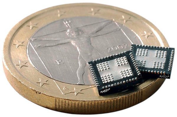
The new Martin Prebump set 03.1, on which patented Hotprint technology is based, is especially designed for the solder paste supply to a small quantity of fresh QFNs placed on a board for the first time. Hotprint delivers the prebumping of QFNs in high quality and reliability down to fine-pitch structures of 0.4 mm, to device dimensions of up to 14 x 14 mm and for an IC pincount of a maximum of 200 pads. Until now reliable prebumping was only possible down to 0.5 mm pitch structures.
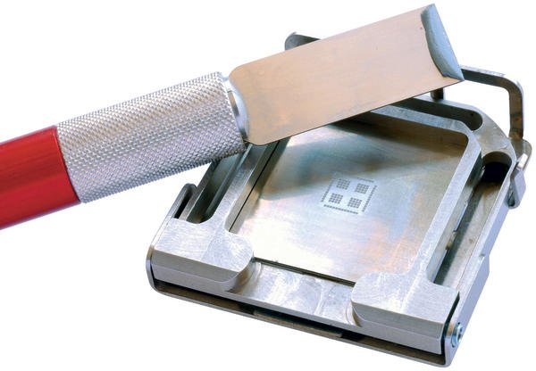
Here, a mini-stencil featuring the appropriate apertures for the QFN is placed and slightly forced on the top of the component in a mini-stencil holder, called the Hotprinter. After this step the paste is supplied and spread across the mini-stencil manually with a small blade or squeegee. In contrast to other similar methods the stencil will not be removed in the Hotprint process after paste print, but rests on the QFN during reflow which helps to maintain an excellent shape of the printed solder structure. This concept delivers the most effective solution above all other prebumping methods at very low costs with high accuracy. The handling is very easy and can be done by the normal staff in electronics assembly lines. The Martin GmbH supplies the stencils for QFNs and also frames.
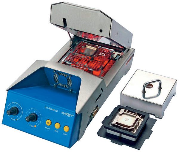
When we look into the offerings from the market we can see that mini-printers, another likely solution, cannot reliably print paste down to structures under 0.8 mm. Also, the lift-off of the mini stencil after the reflow in the Hotprinter prebump mechanism is more accurate and maintains higher precision as the manual release shortly after the print (past can bleed out) seen in other solutions. The QFN package type has virtually no standoff height, and only a minimal spacing of 50 to 70 micron between the PCB and the component is left. Therefore, post reflow cleaning is difficult. It is recommended to use a no-clean solder paste. And due to this minimum spacing, a solder joint inspection after reflow soldering from the component side also cannot be provided in order to verify the process quality. The conventional visual inspection or optical inspection (AOI) of the hidden solder joints beneath the body is of course not possible. Only with costly and time consuming X-ray inspection (AXI) can solder joint verification be completed, but it needs the expertise of a trained inspection operator to evaluate the equipment results. Therefore, for QFNs it is mandatory to deliver an excellent and reliable rework process without any flaws, otherwise production costs will grow remarkably due to the investment in sophisticated inspection instruments. The Martin Prebump-03.1 mechanism, the Hotprinter, is mounted in the controller unit Hot-Reball-03 with compact dimensions of 140 x 290 x 83 mm and a heating power of 50 to 500 W for process temperatures from 210 to 260 °C. A K-type sensor exactly controls the temperature, and programs for eleven different applications are already prepared. An entire typical prebump procedure takes about three minutes. It is noteworthy to draw the attention of users to the fact that the same controller unit can also accept the Martin Reball-03.1 mechanism. This equipment is designed for the reballing of BGAs and CSPs with a pitch of 1,27 mm. With this low-cost rework equipment concept the users can kill two birds with one stone. It is simply a highly cost-effective solution for manufacturing companies with low demand in board rework or reballing of BGA/CSP.
Transfer prebump of multiple components
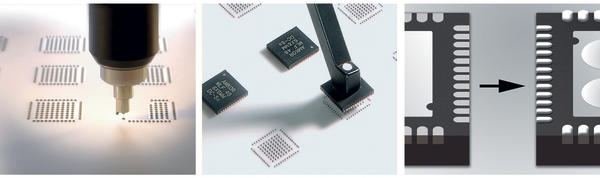
The other method is the transfer prebumping developed by Martin GmbH just a few months ago. It is a fast and accurate method delivering excellent results also down to 0.4 mm pitch (even 0.35 mm and 0.30 mm are possible) which is based on the use of the highly precise Rework Dispenser 05.6 equipment. The innovative and practical process presents the solution in just three steps. First, the dispenser deposits the small dots for the QFN structures on a special ceramic transfer plate. The dots can be as small as 0.013 mm (13 micron in diameter) with a negligible tolerance of ± 3 % only, and up to nine QFN structures can be dispensed in one stroke. The ceramic plane functions as the transfer surface of the mirrored dispensed QFN pad array. In the second step, all the solder paste structures dispensed will be perfectly reflowed to the pads of the then before placed QFNs with the Martin Expert 09 in one run, according to the tested and programmed temperature profile for these components. Then, in the third step, the prebumped QFNs can be used in rework processes easily and reliably. In contrast to the Hotprint method described before, the transfer technique delivers a significantly higher throughput. But due to the needed equipment it demands a higher investment. From this point of view it is a technique ideal for small regular production volumes or higher demand in board rework numbers.
In a nutshell: with the new and patented QFN prebumping technologies developed by the experts of Martin GmbH, fine-pitch structures down to 0,4 mm can be reliably handled, and even 0,35/0.30 mm are possible. Where the Hotprint method is focused on a lower rework demand, the transfer prebumping with its higher throughput is the answer to the request of a greater number of boards. In contrast to other solutions from the market, these prebumping methods are more accurate and therefore the results are excellent and reliable. For a verification of the rework results there is no inspection equipment necessary.
Gerhard B. Wolski
EPP Europe 526
The QFN and its design and application advantages

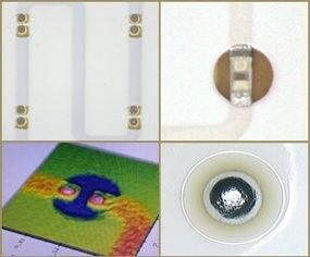
The QFN (Quad Flat No Leads) or from other companies called MLF (Micro Lead Frame) is an often employed integrated circuit (IC) package to be placed on SMT (surface mount technology) board assemblies. This kind of package is similar to the quad flat package (QFP), but in contrast to this the leads do not protrude from the sides of the package. This is a near-CSP (chip scale plastic) encapsulated IC made up with a planar copper lead frame and wire-bonded I/Os (see image). The perimeter lands (tiny pads on all four sides) on the bottom of the package deliver the electrical contacts to the other board circuitry. Some versions of the package feature an uncovered thermal pad which supports thermal enhancement by having the die exposed to the PCB surface, providing a better heat transfer path when soldered directly to the PCB. A direct heat dissipation path is achieved by via holes to the electrically appropriate thermal PCB pad, so the silicon die is discharged from excess heat and thus the thermal performance is increased. This heat-sink design improvement also enables stable ground by use of down bonds or by electrical connection through a conductive die-attach material. In principle the body design consists of the silicon die, an attached thermal lead pad, a lead frame made of copper, and a thermally conductive adhesive is used for attaching the silicon die to the exposed heat pad. The I/Os (4 to up to max. 164) of the die are attached to the frame by thin gold wire bonding technology. To date, there are two general types of QFN packages in use: an air-cavity QFN featuring air within the package, and a fully encapsulated plastic-molded QFN with minimal air voids and no cavity within the package. Each package type has its own benefits. Due to its inner structure, the fully plastic-molded QFN is typically limited to RF applications up to about 3 GHz. It is usually composed of just two single elements, a plastic compound and a copper lead frame, and does not need a lid. In contrast, the air-cavity QFN is usually made up of three elements: a copper lead frame, a plastic-molded body (open, not sealed), and either a ceramic or plastic lid. This version is usually more expensive due to its design, and can be used for highest frequency/microwave applications of up to about 25GHz.
In general, the QFN component offers a variety of benefits including reduced lead inductance, a remarkably small sized “near chip scale” outline, very thin profile and low weight. Maximum height is from 0.6 to 1.5 mm and body size from 1 to 12 mm. The packaging results are significant: thin profile and superior die-to-body size ratio. Since it uses perimeter I/O pads, the PCB trace routing is made easy, and the exposed copper die-pad technology offers good thermal and electrical performance. However, the parts do not come with the usual very small Pb-free solder depot just enough to place and reflow solder it once, so for rework and repair fresh solder alloy is needed. Its engineering and economical features make the QFN an ideal choice for many applications where size, weight, and thermal and electrical performance matter. And in relation to CSP, for example, the pricing reveals better conditions. Also multi chip package and stacked die configurations can be designed based on this IC technology. (GBW)
zusammenfassung
Auf neue QFN-Bauteile muss bei der Board-Reparatur ein ausreichendes Lotdepot aufgebracht werden. Dafür steht zum einen der kostengünstige Hotprint für geringen Durchsatz sowie für größere Rework-Volumen ein Transfer-Verfahren zur Verfügung. Entscheidend ist, dass der Prozess mit höchster Zuverlässigkeit und Präzision ausgeführt wird, denn die Lötstellen sind nicht mehr visuell zugänglich.
Le développement de la technologie prebumping apporte une méthode solide sur le marché de la réparation des boîtiers QFN fine pitch. Grâce à la plaque de transfert en céramique, puis à la refusion effectuée, le prebumping permet une réparation facile des boîtiers QFN. Et ce même pour les futures trames : 0,5 mm est le standard actuel, 0,4 mm est déjà disponible de série sur le marché, 0,35 à 0,30 mm est encore à venir.
Lo sviluppo della tecnologia del prebumping ha messo a disposizione del mercato del rework di QFN fine pitch un metodo accettabile. Con l’utilizzo della piastra di trasferimento ceramica e il successivo reflow, il prebumping consente di riparare facilmente QFN. Questo addirittura anche per passi futuri: 0,5 mm è lo standard attuale, 0,4 mm è già di serie sul mercato, 0,35–0,30 mm è l’obbiettivo futuro.
Share:


