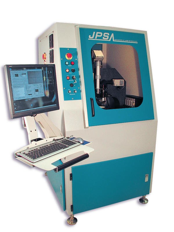
The patented Chroma-Dice UV-DPSS laser systems from J. P. Sercel Associates can now scribe and dice 300 mm silicon wafers up to 500 microns thick. These systems use a fast, low-stress UV laser singulation process that increases yields by reducing debris and post-cut chip breakage. This is thanks to the fact that, unlike mechanical dicing, the UV singulation process is vibration-free. Saw-generated vibrations can generate significant chipping and micro-cracks in the wafer as well as unacceptable cut quality and poor die-edge fracture strength.
The company’s Chroma-Dice systems feature high-performance, ultra-precise air bearing stages that provide higher speed and acceleration in addition to greater travel for wafers up to 300 mm. The system is also available with either 355 nm or 266 nm high-power, short pulse UV lasers for high speed, high yield processing of a range of materials as well as sapphire, silicon, and GaAs wafers.
The systems are available with complete wafer handling systems including cassette loading. An upgraded laser diode wafer edge detector is available for all wafer types. This module interfaces with the new motion control system and allows any type of wafer, as well as partial wafers, to be processed on standard dicing tape frames with no damage to the dicing tape, thus allowing breaking and stretching for pick and place die transfer.
According to the company with this larger wafer handling capability, customers can achieve increased process efficiency, even on thicker wafers. Since the heat-affected zones are minimised, cuts are clean and stress-free, so die count per wafer is higher than with traditional scribing methods, and economic payback is improved thanks to yields in excess of 99 %.
The products and services include UV excimer and DPSS laser micromachining systems, UV and VUV laser beam delivery systems, UV laser materials processing development, optical damage testing, and excimer laser refurbishment services.
EPP EUROPE 467
Share:


