One of the centrally located places in the Havelland region some 40 kilometers north of Germany’s capital, Berlin, is the city of Nauen where PacTech has its headquarters (HQ). The company, founded as a spin-off of the federal scientific Fraunhofer Institute for Reliability and Microintegration IZM in 1995, provides high-quality, expert manufacturing services and production equipment in the fields of advanced wafer level packaging (WLP) and wafer bumping. With subsidiaries in the U.S. and Malaysia, the corporation supplies its outstanding solutions in these relevant business regions.
PacTech – Packaging Technologies GmbH, Nauen/Germany
PacTech’s HQ was established in Nauen in 1997, has continually grown, and the company is to date the biggest high-tech employer in this region with a staff of some 150 people. In the U.S. subsidiary there are another 20 employees, and in Malaysia around a further 110 personnel. The Japanese trading house Nagase & Co. became leading co-partner by taking a major 60 percent stake in 2006, and over the following years this share has risen to a significant 97.2 percent, rendering it the dominant share holder working in close collaboration with PacTech. The product portfolio encompasses comprehensive manufacturing services for wafer level bumping and packaging processes as well as for advanced machinery and plant engineering.
Global presence
In Europe, the U.S. and Malaysia, the full enterprise portfolio of different manufacturing services is available, as well as all of the backend solutions. The equipment engineering is located at the German HQ. All machinery, which is provided and installed globally, stems from the headquarters and carries the well-known brand Made in Germany. The company’s main target area is now the Asian markets, which consume the lion’s share of products and services, according to Thomas Oppert, Vice President Global Sales & Marketing. Therefore, it is no surprise that the headquarters is home to the largest service center, with the biggest clean room environment and equipment manufacturing floor. “One reason for our global presence is the fact that our customers in Europe and the U.S. have increasingly moved their production facilities to Asia,” states Thomas Oppert. “In this respect we have to make provisions so that we can supply our projects, advanced equipment, services and processes in the most best possible and reliable way. In principle, our U.S. subsidiary is responsible for the market in North America, and likewise the Malaysian branch for the whole Asian region including Singapore, China and Taiwan, etc.”
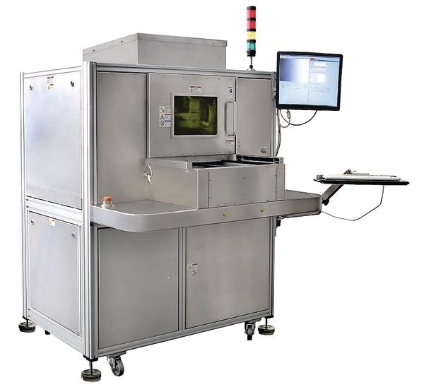
The company employs its own designed and built advanced equipment of course for the most part of the manufacturing services offered, so for electroless wet chemical deposition, the deposition of solder bumps and for plasma cleaning, too. And PacTech’s own compact special reflow ovens are used as well. Any machinery needed in addition to this is second-sourced from other reliable suppliers. Be it in Germany, the U.S. or Malaysia, at all these sites there are identical manufacturing lines or equipment in comparable clean room environments for the main packaging processes. This enables the company to maintain the greatest possible flexibility in all its business regions and to rapidly transfer orders to and from its different sites when necessary. One clear advantage is that processes can be reassigned very easily and reliably among the sites, and the global customer will always receive a high-quality PacTech solution.
A further clean room environment with a second fully automated line for electroless deposition has just been installed in Malaysia. The PacLine is a wet chemical system for the electroless metalization of Ni, Pd and Au on wafer structures featuring high throughput of up to 600,000 wafers (8 inch/200mm) per year. The equipment has an integrated automated robot handling system for wafer carriers providing an economically priced solution for high-volume wafer bumping. At the German headquarters, however, the thinning of 300mm wafers or the backside metalization of wafers has been neither necessary nor viable up to now, as all these services are provided at the Malaysian subsidiary. Interesting is the business relation of services and machinery at the different sites: in Germany 75 percent is equipment, 25 percent services, yet in Malaysia, where equipment Made in Germany is also sold and installed, the relationship is 8 percent equipment compared to 92 percent for services; in the U.S. the shares of both commercial activities are practically equal.
As the PacTech business in Asia is steadily growing, a demo center in Taiwan and another one in Shanghai will soon be opened this year, at the beginning with three characteristic pieces of PacTech equipment: an automated production solder jetting system (SB2-Jet), a jetting machine (SB2-M) for prototyping, and a compact reflow oven (RFA-300). As usual, these advanced machines are engineered and built to the highest standards at the company’s German headquarters. Both demo centers will be ready for use at practically the same time, providing local customers with a number of additional benefits. For example, prototype products will no longer have to be sent from China to Germany for evaluation or customer tests but can be done locally, both quickly and easily – as far as subsequent standard manufacturing processes are in focus.
Wafer level packaging excellence
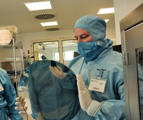
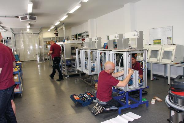
Wafer processing has to take place in clean room environments, which is self-explanatory considering the very delicate nature of these products. The staff working in these special surroundings are fully equipped with particle-free protective clothing, hood, mouthpiece, gloves and all other necessary clean-room gear; and as usual precautionary measures have to be taken prior to entering such rooms. Even particles not visible to the naked eye or simply a minute human hair can destroy chip structures in the nanometer range and therefore damage the product’s quality and reliability. All equipment used for the secure, reliable and appropriate high-quality processing of PacTech’s advanced wafer level packaging is located in clean room environments. Besides the deposition on wafer chip structures, and the laser jetting of single solder balls or the solder bumping of complete wafers, the corporation offers even more advanced manufacturing services such as wafer level and backend processes. These are: sawing or thinning of wafers, backside laser marking, wafer backside metalization, flip-chip assembly and chip singulation. According to market requirements, wafers with diameters of 100mm to 300mm can be processed where larger wafers contain, of course, a higher number of dies. In order to fulfill high throughput and miniaturization demands, automated handling systems have become the norm in volume manufacture. And for the assurance of quality and reliability modern test and analyses systems are employed by PacTech in order to monitor the production and likewise to support the design processes by feedback information. With special semiconductor metrology instruments extra wafer and chip inspections and tests can also be provided.
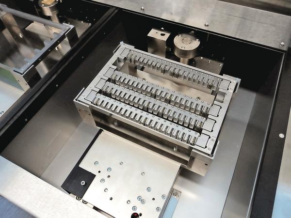
One of the outstanding solutions in the wafer bumping field might now be PacTech’s machine platform SB2-SMs, which comes with a collection of special innovative features. The new system has been developed as an answer to the demands of high-speed soldering of camera modules for smart phones. Here, semi-automated loading and unloading is conducted by a drawer system that can be fitted, with or without retainers, for camera modules which are now widely used in mobile electronic gadgets such a mobile phones, tablets, etc. – and the equipment can be therefore very flexibly utilized in production. The maximum working area of such a drawer is 180mm in length, 150mm in width and 60mm in height. Together with the precise axis system driven by piezo linear motors these attributes allow for the automation of processes which have been done manually until now.
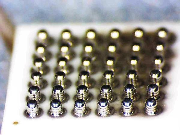
The system places solder balls in all necessary alloys with diameters ranging from 40 micron to 760 micron with a rate of a maximum of 10 spheres/second. The laser-based solder jetting method offers the advantage of combined reflow soldering at the same time, so two processes become one procedure. This saves not only time and money in manufacture but also reduces the costly footprint caused by machinery on the clean room production floor. The fluxer that is normally necessary for soldering needs is no longer applied in this process, resulting in a further saving of material, time and money. This allows electrical contacts to be created instantly, easily and with great precision through laser-based soldering, whether on camera modules for mobile devices such as smart phones and tablet computers, on PCB assemblies for hard drives, or on different 3D-devices. The machine configuration can be cleverly adapted in order to efficiently manufacture other products according to changing user requirements.
In a nutshell: the company is not only a one-stop shop for innovative, expert turnkey solutions for advanced packaging equipment focused on wafer bumping, laser bonding and wafer level packaging; its bumping services are also of the highest quality. (dj)
Zusammenfassung
PacTech, mit Sitz im brandenburgischen Nauen, bietet im Bereich der Mikroelektronik Dienstleistungen sowie Equipment in hoher Qualität rund um das Wafer Level Packaging und Bumping. Um dem Trend von Kameramodulen für Smartphones zu begegnen, wurde eine Maschinenplattform für schnelles Löten entwickelt. Ein Wettbewerbsvorteil, denn manuelle Prozesse gehen fortan automatisiert von statten.
La société PacTech dont le siège est situé dans la région du Brandebourg à Nauen, propose des prestations de services dans le domaine de la micro-électronique ainsi que des équipements de grande qualité pout tout ce qui touche au Wafer Level Packaging et au Bumping. Afin de satisfaire à la tendance actuelle des modules de caméra pour les Smartphones, une plateforme de machines a été développée pour des soudures rapides. Un avantage par rapport à la concurrence, car les processus manuels sont dorénavant automatisés.
Share:


