


When a global provider of air traffic, navigation, and landing system solutions began implementing their next-generation system, limitations of an existing test and debug methodology directly impacted their bottom line. This article describes how Jtag boundary-scan testability was quickly added to an existing product to greatly reduce test and debug time. The boundary-scan methodology is described along with the software tools and hardware required for implementation, hardware design considerations, as well as software modeling and test methods.
Keith Wetterquist, JTAG Technologies, Stevensville (USA)
Air traffic systems must be designed and built to maximize safe and reliable operations and meet stringent requirements of regulatory agencies, while minimizing life-cycle costs over the service life of the equipment. Additionally, these products must satisfy challenging and diverse operating requirements and terrain. Because of these requirements, testing must be thorough and complete.
More efficient test methods needed
With low production run volumes, the complex systems required sophisticated testing by knowledgeable technicians and engineers. As next-generation technologies were implemented, the complexity of the systems increased, as did the test requirements. With the increase in complexity, test and debug time increased, as well as overall product costs for a surveillance processing system. The processing system board is comprised of a 32-bit embedded processor, flash memory, a field programmable gate array (FPGA), analog-to-digital converters, amplifiers and buffers. Analog RF signals from an aircraft approaching an airport enter the board to be digitized and are sent to the FPGA for conditioning and pre-processing. The FPGA then sends the encoded information to the processor. Under the existing test procedure, after a production run of the boards, each one was visually inspected at the manufacturing site. To ensure proper performance, sophisticated equipment and highly-trained technicians were needed. Instead of providing these resources at the manufacturing site interconnect testing and further debugging were performed in-house. Upon receipt of the boards, a technician again performed a visual inspection and began a thorough testing process that would typically last two hours. Next, each board was manually probed to check resistive values in order to identify any problems that could not be found with visual inspection. Then, power was applied to check voltage levels. Once a board was successfully powered up, programming the flash memory was attempted. If the flash programming was unsuccessful, an emulator and simulator were used to troubleshoot and identify the source of the problem. Previous product experience indicated that the problem might be in a buffer, the processor, or the flash itself. Once the flash memory was operational, the board was then put in a cabinet containing a test model of the complete system for functional testing. If a board did not pass these cabinet tests, the board was removed for troubleshooting. Engineers would perform exhaustive calibrations and measurements with sophisticated simulations designed to thoroughly exercise functionality and register accesses. Problems discovered at this stage were often interconnect issues such as shorted or open nets. Sometimes, debugging one board would take several hours due to the complexity of the surveillance processing system. Eventually, all of the boards would be repaired and become fully functional using this test and debug methodology, but the costs in manpower were significant; a new approach was needed.
Test challenges with a Boundary-Scan solution
Problems discovered on the processing system and other products had been difficult to visually or manually identify. Yet, once a problem was diagnosed, it was often a simple repair to correct an open or shorted interconnection or a cold-soldered connection. In-circuit testing (ICT) could automate these kinds of checks, but a costly test fixture would need to be developed for each board type and due to increasing board density, access to all test points was not assured. The costs for test fixtures were prohibitive with respect to the low volumes of manufacturing production runs, and any engineering change order (ECO) on the product would require the development of a new or modified ICT test fixture. Further, manufacturers that serve low-volume product runs such as those for this processing system typically cannot justify investment in ICT systems and as a result, ICT is often not a suitable solution.
The connectivity problems discovered while testing and debugging the boards, however, were exactly the types of problems that the Joint Test Action Group (JTAG) had in mind when developing the IEEE 1149.1 boundary-scan testing specification. As designed, the surveillance processing system contained two boundary-scan Test Access Ports (TAPs), one for in-system programming (ISP) of the flash memory and the other for functional access to the processor and the FPGA. Although the ProVision tool can provide full boundary-scan testing for multiple-chain configurations, there was an additional desire for a single boundary-scan chain to maximize throughput. This would allow for simultaneous testing of four boards using a 4-TAP QuadPOD. Therefore, a creative approach was adopted to combine the two chains into one.
With the product boards already built, an ECO to re-design the board was too costly and time-consuming. To create a single boundary-scan chain without an ECO on the product board, a separate test board was created that would effectively connect the two boundary-scan chains into a single chain. The test board’s main component was an FPGA with an on-board SPI (Serial Peripheral Interface) I2C EEPROM (electrically erasable programmable read-only memory). The FPGA, programmed by the EEPROM, provided both the physical connectivity and control logic required to create a non-conventional implementation of a boundary-scan series loop. The test FPGA could also be used to enhance the testability of the board which is described later.
Once modifications to allow for boundary-scan test were in place for the surveillance processing system design, software tools and hardware controllers were required to implement the boundary-scan test solution. A tool was needed that would utilize the design data from their existing design flow. ProVision met the need, importing the following design data with no modifications:
- the board design netlist, created using the Altium P-CAD PCB (printed circuit board) design entry tool,
- Boundary Scan Description Language (BSDL) files for each JTAG boundary-scan component,
- models for all non-scan devices, most of which were available in the library provided with the JTAG ProVision tool, and
- IBIS (Input/Output Buffer Information Specification) models for the buffers.
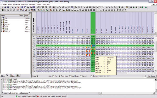
BSDL files, supplied for each part by the vendor, describe the boundary-scan capability while models from the ProVision library describe the non-scan components. The model for an analog-to-digital converter, not in the library, was created using the ProVision model editor using the device datasheet as a reference. Once the necessary design data for the processor board was imported and entered, the ProVision application generators analyzed the design netlist in combination with BSDL descriptions for the boundary-scan devices. Based on this information, a scan-chain topology was automatically constructed. Using models for the non-scan devices, the tool created a board application for optimum test coverage and ISP performance while providing safe conditions on all the board components. To ensure safe conditions, it identified nets with possible driver conflicts as potentially hazardous. Using the ProVision NetExplorer, the test engineer reviewed the nets that had been identified by the tool with potential driver conflicts. Based on knowledge of the design, the engineer overruled any unnecessary controls, which allowed additional nets to be included in the test and resulted in increased test coverage.
The JTAG Technologies JT 37×7/TSI (triple-serial interface) controller and associated 4-TAP QuadPOD provided the communication between the boundary-scan system and the target board. The controller in this application communicated with the PC via a USB (Universal Serial Bus) interface. The four ports on the QuadPOD directly connected to TAPs on the target boards.
Design-for- test considerations
During the implementation of a boundary-scan test methodology for the surveillance processing system, several good design practices became clear. There is no standard for a JTAG TAP connector except that it contain suitable connections noted by the IEEE 1149.1 specification. It is recommended, however, that a consistent approach is used in all designs, i.e. keep pin assignments the same for all projects to allow re-use of connecting cables. To avoid issues with clock skew of the TAP TCK signal and signal integrity on all the TAP connections, it is recommended that the connection between the boundary-scan hardware controller and the board be no longer than 6 inches. To ensure good signal integrity, it is also recommended that the TAP inputs—TCK and TMS, in particular—are buffered at the TAP connection on the board. One or more extra TAPs should be considered as additions to a boundary-scan design for redundancy. If something in the boundary-scan chain is not operating properly, the entire chain could become nonfunctional. By using jumpers to a secondary TAP, a critical component such as a boot-up FPGA, could be isolated and accessed separately if another component in the scan chain were broken.
With the new boundary-scan test system in place, it was time to test a new lot of boards. Boundary-scan tools and hardware had eased the implementation such that the boundary-scan testing could be performed directly at the manufacturing site. After each board was powered-up and the hardware controllers were connected, the boundary-scan checks took less than 10 seconds per board. At the end of the test, ProVision generated a detailed fault report and execution log for each board. The fault report was then interpreted by the company’s Boundary-Scan Diagnostic (BSD) module, which displayed pin-level diagnostic messages giving the specific location and nature of any failures. One short, for example, was found between two data lines on the memory that would not have been found with visual inspection. Prior to implementing the boundary-scan methodology, sophisticated low-level software and an emulator were utilized to identify problems, something that could only be performed by a skilled software engineer. Now, ProVision was used to automate these tests and enhance the use of cutting-edge test methodologies. A problem is identified, located, diagnosed and repaired before the board leaves the manufacturing site. After the tool indicated that the initial interconnectivity test passed the processor programmed the flash memory and the FPGA on the processor board, while the FPGA on the test board was programmed using an SPI EEPROM. Both FPGAs and the flash memory, however, could have been programmed through the boundary-scan chain as well.
Implementing boundary-scan testability on a product that had already been designed required a creative solution. A secondary test board was developed to facilitate implementation of a single boundary-scan chain, in effect connecting the two former chains in series. One benefit the secondary board provided was a way to externally connect and check the primary inputs and outputs (I/O) of the processor board. Using bidirectional buffers on the test board and controlling the output enable (OE) of each I/O buffer with the test board FPGA, the direction of the data flow could be controlled. By dynamically controlling the flow of data, external connections on the board were driven and checked. Boundary-scan tests checked the interconnectivity between the JTAG boundary-scan components and additional checks on the primary I/O provided increased product testability. Another test enhancement for the boundary-scan test flow was the addition of a simple check of the flash memory. Using the boundary-scan chain to fully test a flash memory would be inefficient. Other tools specifically designed to do that task would be a better choice. However, leveraging the control and connectivity of the boundary-scan chain to do initial checks on the memory was very easy to implement, and it could quickly determine whether or not the basic functionality of a memory was working. By simply writing and reading back a very small file to the memory, checking the memory control lines and data interface was automated through the ProVision interface.
Manufacturing portability and flexibility
As previously mentioned, a functional boundary-scan test process was set up at the manufacturing site. Before any board left the manufacturing site, most problems were identified and repaired. Implementing a boundary-scan test system at the manufacturing site removes the excessive cost of shipping boards back and forth between the project team and manufacturer for testing and repair. Also, the portable nature of a boundary-scan test station allows it to be set up at any manufacturer that the system company chooses. In using a company’s hardware controller with a 4TAP QuadPOD and with the secondary test board, four boards can be tested simultaneously and independently. A boundary-scan test methodology resulted in a significant reduction in the time technicians and engineers invested in testing, diagnosing and repairing boards. Initial test times were reduced from greater than 30 minutes to less than 10 seconds. Additional cost savings were realized when boards no longer needed to be shipped from the manufacturing site to the company and then back to the manufacturer for repairs. Considerable savings were realized in engineering manpower that had been required for up-front testing as well as in the time expended troubleshooting hard-to-diagnose failures. Finally, because most problems were now rapidly identified, diagnosed and repaired, the production yield for processor boards increased from approximately 30 % to greater than 90 % at the manufacturing site.
As more BGA (ball-grid array) packaged components are incorporated into the company’s air traffic, navigation, and landing system products, visual inspections no longer provide appropriate or reliable results. A boundary-scan test methodology coupled with comprehensive and easy-to-use tools will be critical to identify and resolve connectivity issues. The use of boundary-scan tests will be expanded to provide higher test coverage for new products especially as a wider range of parts and increasingly sophisticated integrated circuits (ICs) become available. With the success of implementing boundary-scan test practices on the surveillance processing system, testability has been given a stronger consideration in the product specification and design phases for future product development and manufacturing.
Zusammenfassung
Boundary-Scan, auf dem IEEE 1149.1 Standard basierend, ist die herausragende Technologie, um Test- und Programmier-Herausforderungen für komplexe elektronische Systeme heute und morgen zu bewältigen. Der Artikel erläutert eine Implementierung dieser Methode.
Le Boundary-Scan, développé à partir de la norme IEEE 1149.1, est une technologie exceptionnelle qui permet de relever les défis que posent les tests et la programmation des systèmes électroniques complexes d’aujourd’hui et de demain. Cet article explique la mise en œuvre de cette méthode.
Share:


