Stacked dies enable highly integrated systems in a single package. As a miniaturized and cost-effective answer to this challenge, SoCs (systems on a chip) have made progress, but they will soon come up against economic limits. This applies particularly with embedded technologies for improved performance, when at least two different process technologies are to be integrated on a chip. This kind of technology mix could be implemented more cheaply and with better performance features through different chips in the most suitable technology for the respective functions. But this is where the next challenge often crops up. Connecting multi chips at board or substrate level leads to complicated routing and interference. A possible solution is the third dimension: stacked dies made of ultra-thin silicon, which blur the boundaries between semiconductor manufacture and packaging.
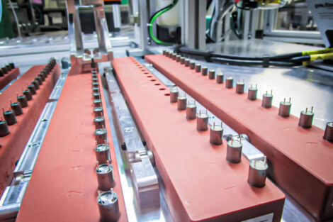
However, the flexible silicon chips used for this have special characteristics which are very demanding in the handling. They are extremely fragile and often warped. Suitable equipment for processing these thin dies must therefore take account of these particular features. Also, with stacked dies, an adhesive tape is often used instead of the conventional epoxy to achieve defined layers of adhesive. To enable the special requirements of the bonding technologies to be met, Datacon has created a flexible machine platform that can be precisely tailored to these technologies. The 2200 apm+ multi-chip die bonder with linear motors and dynamic servo-control, automatic compensation for temperature drift and high-resolution camera systems ensures a positioning precision at the XY level of ±7µm at 3-sigma (s) and a maximum tilt of ±0.15° at 3s. This is especially important for the adhesive technologies that are not as self-centering as soldering techniques are. The Z-axis can be individually controlled for bonding functions and adhesive application, so that, for example, warped substrates can be processed. For assembly on warped substrates, a special ultra-light tool has been developed, whose low bond force works in the range of 0 to 6g (±50mg). The wafer transport processes up to 25 different wafers, for which five ejection tools are arranged in a carousel. Another highlight is the material-protecting synchronous sequence of motions, whereby the chip is picked from the carrier with the help of vacuum. This allows handling of small chips with an edge length starting at 170µm and, for flip-chip assembly, 500µm chips. The automatic tool changer holds up to six different tools, now including a bond head that can be heated to 350°C, which is especial- ly beneficial for temperature-controlled adhesive processes in flip-chip assembly. This feature is crucial for the adhesive technologies, such as NCA, ACA, ICA (for flip chip), and adhesive tapes.
EPP EUROPE 435
Share: