
Consumer appetite for smaller communication devices with increased functionality is growing fast. Although manufacturers can deliver increasingly miniaturised components, the challenge is to do this economically and with higher yield. The requirements of miniaturisation also need to be balanced with those of “standard” technology to achieve heterogeneous assembly. With these challenges likely to be front of mind for electronic manufacturers visiting productronica (Munich, 12–15 November) DEK’s Future Technologies Manager, Mark Whitmore, gives his opinion on how best to tackle the miniaturisation challenge, based on DEK’s latest research.
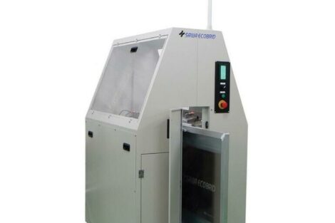
DEK Printing Machines, Weymouth (UK)
Visitors to productronica will be exploring the exhibition looking for technological solutions to a number of challenges. One of these is to deliver smaller components within heterogeneous assemblies and in a cost-effective manner. Consumer trends are pushing towards greater miniaturisation, with smartphones emerging as the primary computing device of choice, with global sales outstripping the PC market.
Today’s electronics manufacturers are increasingly looking for solutions to questions such as: How small can we print? What are the tightest pitches? Can we print small deposits next to large ones for high mix technology assemblies? How closely can we place components for high density products? In addition, how can we satisfy some of the cost pressures through the whole supply chain and improve the production process?
But miniaturisation is nothing new. The 1.27mm pitch Ball Grid Array (BGA) packages that appeared in the mid-nineties represented a significant progression. Today, 0.3mm pitch packages are on the horizon. The feature sizes that are involved would, only a decade ago, have been considered in the Semicon domain. To add to this challenge, the smaller assemblies are also more complex.
Why stencil design is key factor
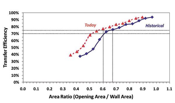
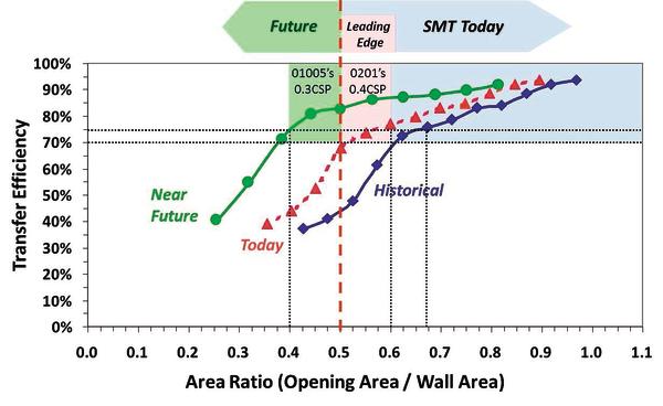
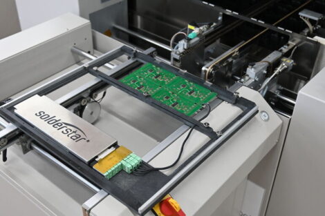
For an assembly community already operating close to the limits of SMT capabilities, scaling stencil feature sizes for shrinking component geometries poses a significant challenge. Stencil aperture area ratio dictates the size of deposit printed. The area ratio rule is the relationship between stencil aperture opening and the aperture surface area. To deliver the next generation of miniaturised SMT devices, this rule has to be broken and doing this will require new processes and tools.
Research has already discovered stencil printing techniques able to address some of the challenges with miniaturisation. For example, active squeegees such as DEK’s ProActiv, have been shown to push area ratio limits to new boundaries, in particular these have been shown to be useful for heterogeneous assembly. This enables the industry’s smallest components to be printed alongside its largest and most complex, using a conventional printing process and single thickness stencil. An increasingly important part of the overall equation is stencil aperture shape and design. This is key if electronic manufacturers are to achieve economic repeatability when delivering smaller components. With this in mind, DEK recently completed a project, resulting in greater effectiveness of a square-designed aperture in delivering paste, and a preference towards an active squeegee process.
The project particulars
DEK’s project looked at opportunities to move the area ratio curve by investigating the impact of various combinations of aperture design, solder paste and squeegee assembly. Theoretically, a square aperture of a given size provides the opportunity to deposit 21.5% more than its circular counterpart and the company’s experiments demonstrated this is also the case in practice. On the question of solder paste particle size, net gain was seen to be at a fairly low level. It is worth pointing out, however, that only one solder paste formulation was tested. The ultrasonically activated squeegee also delivered significant increases in solder paste transfer efficiency, supporting a number of other published investigations. These results tell us that marrying effective stencil design with an active squeegee process will deliver the highest levels of accuracy.
What’s next?
At the company, we are focussed on keeping abreast of the long-term industry trends and challenges facing our customers, and developing technologies in response to these. Customers are already asking us about our print capabilities for 0.3mm CSP assembly, and we believe that 0.3mm pitch CSPs will soon become mainstream production. Once 0.3mm pitch CSP is phased into the high volume segment, we expect to see the 0.25mm and 0.2mm pitch come onto the roadmap of ‘state of the art’ companies.
For these reasons, DEK plans to continue exploring the importance of stencil design to optimise the process of printing for miniaturised components. Please get in touch with us if you would be interested in finding out more, or visit our website to read our latest research.
We also look forward to speaking to you at productronica this year. Uniquely, our booth will include a “Solution Centre”, where DEK’s Customer Service Group will be on hand to answer any questions you might have about your print process challenges.
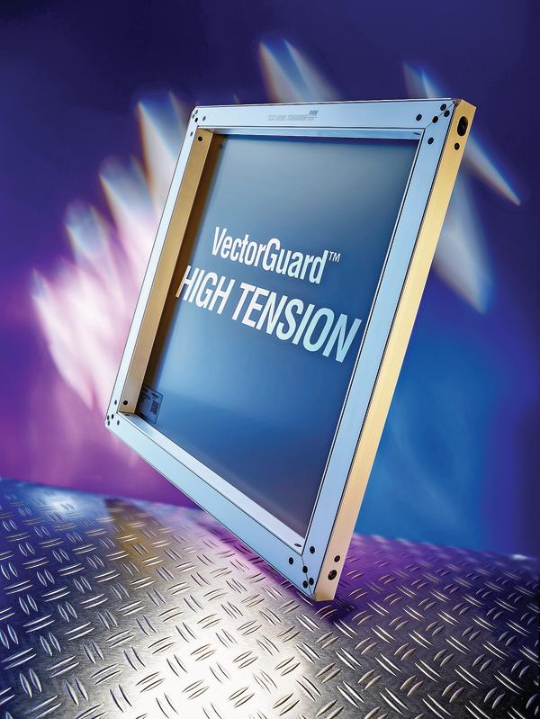
The Solutions Centre will provide the perfect opportunity for you to tackle your printing challenges with the free advice of a DEK expert. The Centre will also feature a schedule of presentations on industry issues to complement our printing platforms in action at the booth, as well as DEK’s Process Support Products (PSP) such as the recently launched, and industry leading VectorGuard™ High Tension stencil system. This stencil system, launched earlier this year, delivers excellent paste deposition and definition, better transfer efficiency for highly miniaturised components and zero tension loss of the life. Furthermore, ProActiv, the ultrasonically activated squeegee which delivered such strong results within the experiment described here will also be on sale. We look forward to speaking to you.
Productronica, Booth A2.405 and B2.225
Zusammenfassung
Der Bedarf an kleineren Kommunikationsgeräten mit noch mehr Funktionalität steigt ständig. Im Hinblick darauf sind die Elektronikhersteller auf der Suche nach Lösungen auch für Fragen rund um den Pastendruck, in Verbindung mit der Miniaturisierung. Wie dennoch ein hohes Maß an Druckgenauigkeit erreicht werden kann, zeigt dieser Artikel.
Le besoin en appareils de communication plus petits avec encore plus de fonctionnalités augmente sans cesse. De ce point de vue, les fabricants d’électronique sont à la recherche de solutions également pour tout ce qui est de l’impression de la pâte, en corrélation avec la miniaturisation. Cet article montre comment il est tout de même possible d’obtenir un haut niveau de précision pour l’impression.
Share:


