Modern power electronics is the key to energy efficiency. Viewed against the background of ever increasing prices for raw materials and energy, and the limited availability of the fossil fuels, it becomes obvious that our society will be forced to expend more care in its dealing with the resources of our planet as it has done in the past. Particularly for those countries that have limited resources of raw materials and fossil fuels, the sustainable consumption of these valuable commodities will gain in importance. The development of alternatively generated energy from regenerative sources, the efficient use of electrical energy, as well as the creation of totally new mobility concepts can only be realized with a high proportion of leading-edge power electronics.
Dipl.-Ing. Juergen Friedrich, Ersa GmbH, Wertheim (Germany)
For those reasons, power electronics has experienced, for quite some time now, an enormous boom. Today, the possibilities that open up through the use of new, high-performance components in combination with intelligent processor controls allow for highly energy efficient controls and systems, frequently in combination with a high integration density. But with this boom of power electronics, some very special challenges surfaced for the designers and for the staff on the production floor.
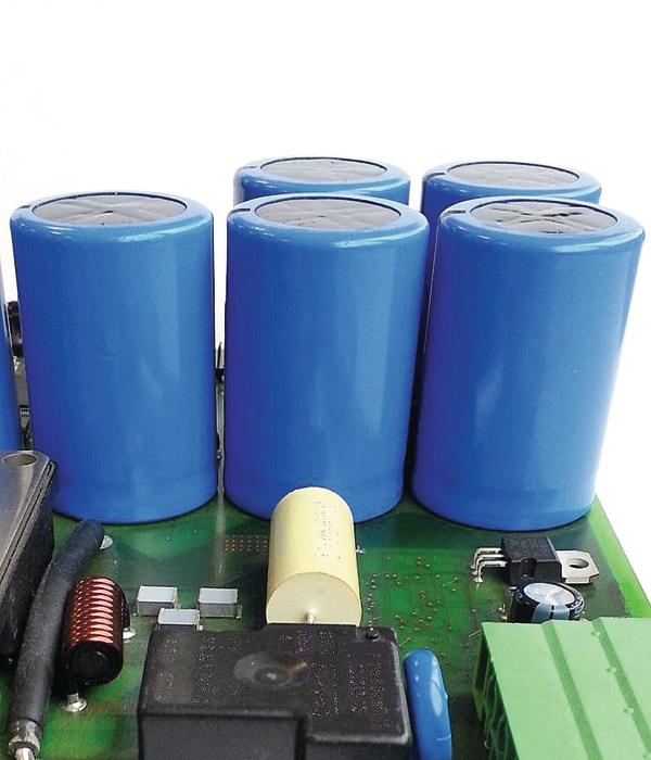
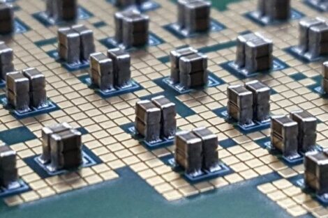
On power electronic assemblies, high currents have to be handled which, due to physical constraints, necessitate larger than usual cross sections of the conductor paths. Similar applies to the cross section of the connection pins of power components such as semiconductors, chokes, electrolytic capacitors, etc. For the printed circuit boards, the usual copper thickness of 35–70µm for the tracks is no longer sufficient. For power electronic applications, PCB technology offers today multi-layers boards with inner layers of up to 4 x 400µm and outer layers of up to 2 x 100µm, with a total thickness of 4 to 5mm. In cases where the thickness of the copper layer is not sufficient to handle the current, heavy bus bars, which need to be soldered to the PCB, have to be used. A common mistake repeatedly being made is that during the design of the PCB, the basic design rules for standard components of little mass are also applied for the heavy solder joints of power electronic components. What is represented on the CAD system of the designer as a simple connection point is actually a solder joint possessing a very high heat capacity. This has to be reduced to a minimum, if the demands placed on the solder joint are to be met without damaging the PCB during the soldering process.
Demands for the assessment of solder joints
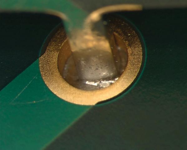
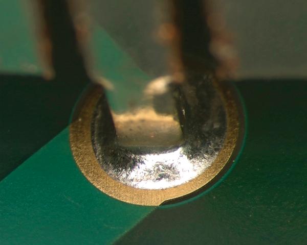
To ensure the reliability of such solder joints and to allow for an accurate visual assessment, the minimum requirements placed on the solder joints can easily be defined. The rise of the solder in the through-hole should be 100% and, very importantly, a fillet should be visible on the portion of the pin extending above the board. If these criteria are achieved, visual inspection of the solder joint is a safe procedure, and there is no room for interpretation.
In practice, though, confrontation with the specification of IPC A610 arises, which considers – for class 3 assemblies – a rise in the through-holes of 75% as sufficient. This definition poses great difficulties for the visual inspection, since how can you judge, sitting at a microscope, whether a capillary rise is indeed 75% of a plated through-hole? This judgment is exclusively dependent on the subjective impression of the inspecting employee, since it is not directly measurable and therefore subject to a large tolerance range. To eliminate this uncertainty, the demand for a 100% hole-fill has been implemented as the rule. If the capillary rise of the solder in the plated through-hole is less than 100%, there is the danger that the pin of the components may not be fully wetted. Through this non-wetting, the cross section of the solder joint through which the current flows is reduced. If a high current flows through such a solder joint, a voltage drop can be observed. This power dissipation causes the solder joint to warm up, a condition which in turn raises the resistance and increases the power dissipation in the solder joint even further. In the worst case, this can lead to the thermal destruction of the solder joint and to the complete failure of the board assembly.
Layout of solder joints in power electronic assemblies
After having defined the demands placed on the solder joints, the next step is to clarify which technical rules should be used when designing the solder joints, and to establish which of the two available solder processes and which parameters should be used.
To even have a chance to achieve the required fill of the plated through-hole, it will be necessary to reach, both at the copper pad on the top side of the board and on the pin of the component, a temperature which is higher than the melting point of the solder alloy used. For lead-free solders, this temperature is in the range of 245°C or higher! Only if this condition is met, the requirement for wetting being able to occur is fulfilled. This means, that within the few seconds of the soldering cycle an appropriate rise in the temperature of the board and on the component lead has to take place. The transfer of heat which leads to this rise in temperature is effected in two steps during the process. During preheating, the board assembly is being heated up to a basic temperature level, from where, in a second step, the liquid solder of the wave adds the still missing amount of heat. From this it is obvious, that for the soldering process the preheating function is of immense importance, and that the additional use of upper preheaters can assist to ensure a uniform and effective heating of the upper side of the board as well as of components such as chokes and bus bars.
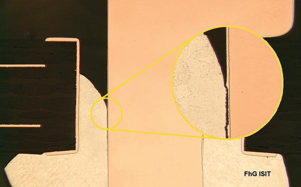
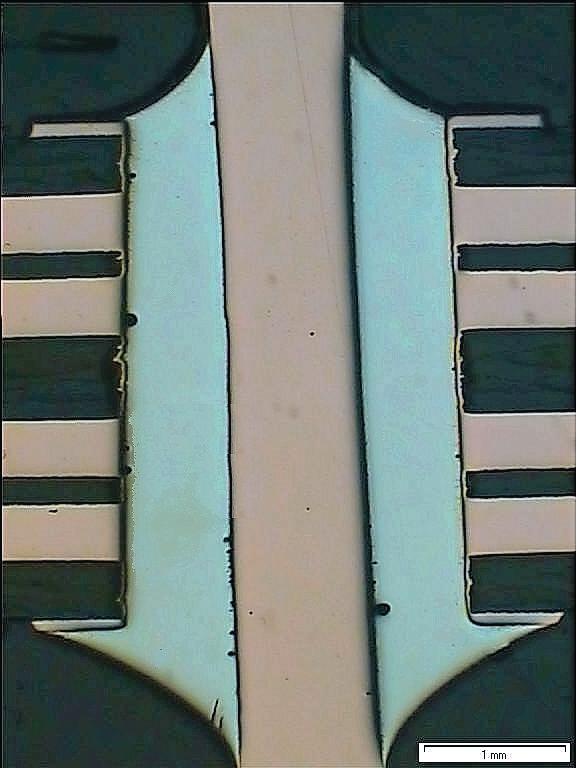
When the liquid solder of the wave contacts a pad on the board, the solder rises in the capillary gap between the plated surface of the through-hole and the component pin. In the process of rising, the solder transfers its heat to the wall of the through-hole and the pin, heating up the wall and the pin. The excellent heat conduction characteristic of the copper allows the solder to rise up the upper side of the board. A crucial parameter is the dimension of the capillary gap between the plated through-hole and the pin. The larger that gap, the larger the volume of solder able to rise, and therefore the larger the amount of heat transferred to the barrel.
If the barrel of the plated through-hole is connected to a heavy inner layer, then the thermal energy delivered by the liquid solder quickly flows to the inner layers. This heat lost is no longer available for heating the remaining length of the barrel. As a result, the solder in the barrel cools down and eventually solidifies before it has reached the surface of the board.
To minimize the cooling of the solder, it is imperative that the barrel be thermally decoupled from the copper layer, without weakening the current load capacity of the connection. The usual way to achieve this is to add heat traps to the layout. Heat traps reduce the cross section at the solder joint through which the heat is lost, reducing the amount of heat lost and therefore raising the temperature more quickly. With the capillary gap and the heat trap, the PCB designers have available two very effective parameters. The quality and the manufacturability of the solder joints on a PCB are contingent on their correct application!
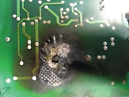
There are, unfortunately, components which cover – similar to a heat shield – the pad of the solder joint on the top side of the board. A typical example of such a component would be the electrolytic capacitor, which shields the area to be soldered so thoroughly, that even the effect of heat generated by a top side preheater directed at the upper side of the board becomes negligible. The large and bulky component bodies shield the solder joint so well, that the total thermal energy required for the soldering process has to come from below into the board assembly, to be transferred through the board to the top pad and the pin. In cases such as these, it is recommended that thermal vias, with which additional heat can be transferred to the top, be provided. In practice, these thermal vias are placed around the plated through-hole and integrated into the pads of the respective solder joint. During soldering, the solder rises, unimpeded, through the thermal vias to the top of the circuit board. This additional thermal energy leads to a faster heat up of the plated through-hole on top of the board, and makes available more thermal energy to heat up the pin of the component. By now it should have become apparent that the layout of the board has considerable influence on the quality of the solder joints. If this knowledge is not taken in account during the design of the board assembly, it can lead to serious quality deficiencies during production. Serious layout defects may cause the assembly to be virtually impossible to manufacture. In those cases, it is frequently attempted during production to compensate for the deficiencies in the layout by changing the parameters of the soldering process. Most frequently the contact time and the solder temperature are modified. Both these parameters need to be approached very cautiously, as these changes can quickly cause irreparably damage to the base material of the boards. The damage occurs when the decomposition temperature TD of the epoxy resin system is exceeded. In practice it is noticed that on the production floor the TD of the board material is rarely known. Added to this is the specification of the board material, which, as a rule, is based on 288°C. For the soldering process, this means that the temperature range between 288°C and the TD in relation to the soldering time is not defined! Typical defects that can appear in this temperature range are retreat of the epoxy resin and delamination of the base material. It is therefore prudent to first attempt to overcome the deficits in the heat management of the board assembly by increasing the preheat temperature, before taking the step to raise the solder temperature to more than 288°C.
The use of solder masks
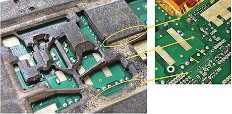
To solder through-hole components on to power electronic assemblies, either the wave- or the selective soldering process may be used. In the selective soldering process, the use of mini-waves is well established in the industry, whereas in wave soldering solder masks are frequently used. This latter process, though, is subject to certain restrictions. Solder masks cover SMT devices mounted on the solder side of the board, leaving exposed only those areas where through-hole component protrude. The ratio between covered area and area exposed for through-hole devices is of significant influence on the heat-up performance of the assembly during the preheating cycle. The smaller the area exposed for the THT components, the more difficult will it be to adequately preheat the assembly. The reason for this is that a very large portion of the heat available will be absorbed by the mask, so that it is not available for the board. Selective soldering with a mini-wave does not necessitate solder masks. Therefore there are no thermal restrictions
A further critical point when using solder masks is the issue of long term reliability of the assemblies. During the application of flux in the wave soldering process, flux can creep into the gap between the board surface and the solder mask. These residues are subsequently covered by the mask, and will therefore not decompose through contact with the hot solder. The interaction of these still active flux residues with small amounts of solder paste possibly remaining from the previous SMT process can lead to reliability issues of the assembly.
SMT Hybrid Packaging
Booth 9-330
ZusaMMENFASSUNG
Die Entwicklung der alternativ erzeugten Energie durch regenerative Quellen, der effiziente Gebrauch von elektrischer Energie sowie die Realisierung völlig neuer Mobilitätskonzepte kann nur mit einem hohen Maß von Spitzenleistungselektronik realisiert werden. Insofern hat die Leistungselektronik einen enormen Boom erfahren, welcher ganz spezielle Herausforderungen an die Designer sowie den Produktionsmitarbeitern stellt. Was es zu beachten gilt, um zuverlässige Selektivlötstellen zu erhalten, lesen Sie im Artikel.
Le développement de l’énergie produite demanière alternative à partir de sources régénératives, l’utilisation efficace de l’énergie électrique ainsi que la réalisation de concepts demobilités entièrement nouveaux ne peuvent être réalisés qu’avec l’aide d’un degré élevé d’électronique présentant de hautes performances. Par conséquent l’électronique performante a connu un grand Boum qui impose des défis très spéciaux aussi bien aux designers qu’aux collaborateurs de la production. Pour savoir ce qu’il convient de respecter pour préserver des points de soudures sélectifs fiables, veuillez lire l’article.
Share:


