
Electronics manufacturers face multiple challenges and are constantly under pressure to improve quality, increase yields, increase profitability and reduce wastage. An operational area which can help manufacturers achieve all these objectives is effective elimination of contamination from the SMT production process. This article looks at the impact of contamination, its key causes and effective solutions which can be put in place.
Callum Campbell, Teknek, Renfrew (UK)
Too many manufacturers are still not aware of the impact contamination is making on their productivity and profitability. Even moderate levels of contamination can lead to downtime, wastage and expensive rework. Every manufacturer is striving for zero defects and 100 % uptime. Eliminating contamination from production is a prime element in achieving this.
At a SMT industry conference last year one of the sessions focused on aspects relating to high performance cleaning in the assembly process, for example in-line aqueous cleaning equipment and solvent centrifugal cleaning. The programme introduction to this section stated – “Cleaning challenges have increased with the growing complexity of electronic assemblies, miniaturisation, alloys, board finishes, lower component gaps and improved flux designs. The need to remove ionisable contaminants is critical to production yields and reliability.”
This subject will not be new to anyone and improving yields is paramount to many companies success or survival, however the cleaning technologies discussed at the conference only covered cleaning during the assembly process and did not consider cleaning of the bare PCB board at the very start of the process, prior to solder paste print stage, where large quantities of particulate contamination can be introduced into the production line.
Moore’s Law suggests we can expect the technological demand for smaller and more compact circuitries to continue and as these drivers increase we therefore need to consider the impact of even the smallest particles of dust throughout the process but especially at the start, before solder paste printing.
Bare board cleaning
The SMT industry overlooks the important opportunity to start the assembly process with a cleanest possible product, despite widely accepting that around 60 % of faults throughout the manufacturing process are introduced at the print stage. There is a mis-conception that boards are supplied spotlessly clean, however in truth this is seldom the case as boards are not packaged in cleanroom environments. They are then loaded onto planes, trains, automobiles or container ships and transported thousands of miles around the world; before being opened (in another non cleanroom environment) and stacked onto board loaders, fed into cassettes or manually handled onto printing machines. At each of these stages there is ample opportunity for the boards to become contaminated.
Another technological driver is the increasing use of “greener/lead free” materials. Newer solder pastes have different melting points and flow characteristics have changed making the materials stickier. The resultant operating parameters are much narrower and more open to corruption from sources of contamination. In addition, copper has a tendency to dissolve in tin rich, lead-free solder alloys which can happen during repetitive processing of reworked boards and is one if the main reasons assemblers are moving to zero tolerance on rework. Getting it right first time is a key objective, so any possible sources of contamination which might cause rejects or rework at the print stage have to be removed.
Contamination within surface mount assembly causes three main faults – process, solder and reliability. Particulates can enter the manufacturing process at any stage and directly affect the yield. Eliminating contamination improves the solder paste print quality and reliability of the assembled board, improves the efficiency of the production process and improves yield rates.
Eliminating process problems means efficient and effective production, providing faster turnaround and higher profit margins. In PCB manufacture where margins are being constantly squeezed, optimising the manufacturing process can mean the difference between growth or decline. PCB assemblers face the many problems of escalating costs, tighter tolerances, finer pitch and increased customer demands, which is forcing them to re-assess their processes without raising overall manufacturing costs. Contamination on the bare PCB which causes solder paste defects is directly responsible for lower production yields.
Contamination sources and defects
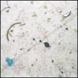
The propensity for contamination is all around in the production environment and particles as small as 25 µm can cause print defects. Typical sources of particles include:
- Hair – the average hair loss for a person is 50 per day (~100 µm)
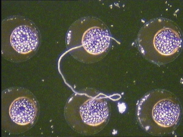
- Lint – cloths are typically used in production environments for wiping purposes. Although deemed to be lint free they can snag when wiped across pad areas or stencils, generating loose fibres. This can be avoided by using higher quality clean room cloths (~50 to 100 µm)
- Clothing fibres – fibres from garments can contaminate the production process (~50 to 100 µm)
- Dust –dust is mostly composed of human skin flakes. On average a person breathes 700,000 skin flakes per day and sheds one layer of skin every 24-hours (~20 to 50 µm)
- Production plant – the ceilings, floors, shelving and packaging materials are all sources of particles (100 to 200 µm)
- Epoxy dust – during the bare board manufacturing process contamination removal systems are used at every step in the process. However, after routing only the top surface can be cleaned. This means the edges will still have loose dust attached. This dust is disturbed during packing and transport and can be a potential contaminant (~20 to 100 µm)
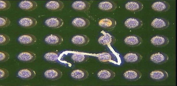
- Glass splinters – PCBs are made from a fibrous substrate posing the risk of loose glass splinters from snap-outs or routing (~10 to 50 µm)
- Solder paste – misprinted boards are frequently wiped clean and sent down the line again – loose solder paste left on the board can cause problems such as solder balls (~10 to 50 µm)
- Solder resist – can flake away leading to contamination (~50 to 100 µm)
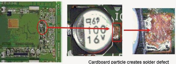
- Packing materials – boards which are individually wrapped in paper can produce paper fibres which attach themselves to the boards by static. Cardboard boxes, when handled, also release swarf into the environment and has been found to create defects (~50 to 200 µm)
- Components – falling onto the bare board.
All the above contaminants can be attached or attracted to the PCB by static. Boards are insulators so will hold a static charge and static is generated during handling and removal of the boards from packaging or loading into feeders or cassettes. Therefore neutralisation of any static charge must also be part of the overall contamination elimination strategy. Research has shown that 80 % of contaminants are introduced into a clean area by people and products, 15 % are generated by the products themselves and 5 % is actually produced by the room and filtration systems.
By way of re-enforcing this point, in a specific production facility test, print operators wore different coloured tee-shirts on consecutive shifts, the first shift wore blue, the second shift wore red, and the third shift back to standard blue shirts. Twelve hours after reverting back to normal blue production tee-shirts, red fibres were still being found in the production environment.
Failure to address contamination issues within the production environment can cause a number of serious problems including:
- Stencil apertures can become blocked by contamination so the print is incomplete
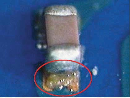
- During reflow contamination in the solder paste can volatilize causing a crater in the solder
- Tombstoning can occur where the chip component stands on end with one end soldered to the board and the other end free
- Fibre from cloths used to clean stencils can become trapped between pads which could lead to short-circuiting
- Poor solder wetting
- Unreliable solder joints
- Dry solder joints
Every time a PCB requires rework the reliability of the board is compromised. Misprinted boards can be washed down and wiped clean but frequently small traces of solder paste (solder balls) can remain on the board.
Contact Cleaning Solution
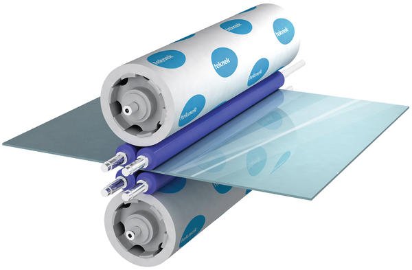
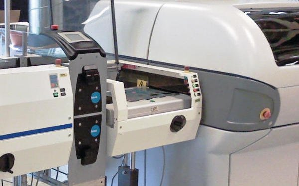
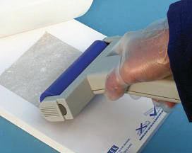
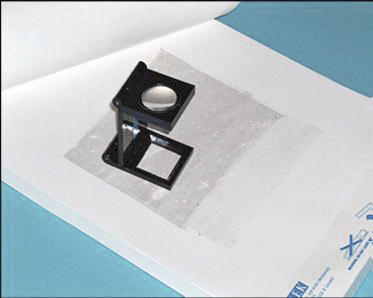
What can be done to combat particulate contamination? The first thing is to ensure high standards of cleanliness are enforced throughout the production site. There should be a scheduled cleaning routine which also includes the thorough cleaning of the production equipment as debris inside the machinery can contaminate the boards. However, it is vital that the PCBs are scrupulously pre-cleaned before they enter the production process. Many manufacturers attempt to do this with brushes, vacuum or blower systems which can remove some of the contamination but not all. A more effective method to prevent particles entering the production process is by using specialist contact cleaning equipment, such as the Teknek SMT Clean Machine. This equipment uses a series of special elastomer rollers which make contact with the substrate. The rollers pick up and remove loose particles down to and smaller than one micron in size. The particles are then transferred to a pre-sheeted adhesive roll for examination, analysis and disposal. The Teknek machine also incorporates powerful anti-static bars to prevent re- contamination of the boards before they enter the screen print stage.
Measurement of the cleaning effect
Automatic Optical Inspection (AOI) -or Solder Paste Inspection (SPI) of boards after the print process is becoming more popular with manufacturers and is showing (amongst other things) how particulate contamination is affecting the board failure rates.
An example shows the overall reduction in board failures after introduction of board cleaning before solder paste print during a three week test period with a Teknek SMT board cleaning machine, measured on a Koh Young SPI system. Overall failure rates fell from an average of 9.5 % to 5 % – an improvement of 47 %. The excessive solder falls from an average of 3.4 % to 1.3 % – an improvement of 62 %. And the bridging falls from an average of 1 % to 0.7 % – an improvement of 30 %. Insufficient falls from an average of 2.1 % to 0.8 % – an improvement of 61 %.
Boards which are pre-cleaned and have undergone static neutralization offer a better surface for printing, improve solder joint integrity and provide better stencil to board gasketing. This means that rework is greatly reduced and the incidence of wasted boards is sharply decreased.
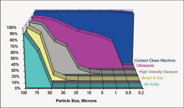
Contact cleaning equipment has been proven to provide board cleanliness levels much higher than brushing, vacuum or ultrasonic type systems as the specially formulated elastomer cleaning rollers make physical contact with the board surface overcoming any boundary layer effect which retains particles within the area of stationary airflow. In addition the contamination collected on the disposable Adhesive Roll can be inspected or analysed to help identify the source of the particles.
Brushing or vacuum systems will often cost less than contact cleaning systems but will leave contamination behind, thus not truly resolving the issue. However, employing effective contact cleaning equipment such as the machine has been shown to dramatically reduce reject rates and provide repeatable and consistently high yield performance.
Conclusion
In summary as the electronics industry strives for zero defects and form factors become ever smaller it is vital that manufacturers put in place powerful anti-contamination strategies to eliminate the impact of contamination and improve yields wherever possible right from the very beginning of their production lines. Starting off with a clean substrate helps increase production yields as residues only become more difficult to remove with thermal and chemical processing.
Callum Campbell is New Business Development Manager at Teknek, the global leader in contact cleaning technology for the electronics and manufacturing sectors. Callum joined the company in 1984 and is now responsible for the development of key strategic market sectors having been involved in various sales and marketing roles, travelling extensively as a regional manager in both Europe and the Americas.
Zusammenfassung
Die Hersteller in der Elektronik stehen immer mehr unter Druck durch die ständig steigenden Anforderungen. Eine Methode, dem gerecht zu werden, könnte in der Entfernung von Verunreinigungen im SMT-Prozess sein. Der Artikel vermittelt einen Einblick auf den Einfluss von Verunreinigungen, den Schlüsselursachen und zeigt effektive Lösungen.
Les fabricants dans le secteur électronique subissent une pression accrue en raison des exigences de plus en plus élevées. L’une des méthodes pour y répondre pourrait être l’élimination des impuretés dans le processus SMT. L’article expose un aperçu de l’influence des impuretés, des causes clés et présente des solutions efficaces.
Share:


