Over the last decade, the adoption of wafer-level packaging (WLP) has expanded to a wide range of semiconductor devices applied in a cross-section of industries from automotive to mobile phone, from sensors to medical technology. This study evidently shows that high-speed-placement using standard SMT (surface mount technology) platforms provides clear advantages in reducing both assembly costs and capital equipment needs. MicroTape, taped & reeled components are easier to handle than wafers or other adhesive-based tape systems providing for less component attrition due to handling problems.
Of the two basic WLP form factors, bare die, requiring gold wire attachment to integrate chip function into a circuit, has typically been used for low-pin-count (< 50 IOs) applications, including analog devices such as power amplifiers, battery management devices, MOSFETs, image sensors, integrated passives, etc. The second form factor, flip-chip packaging, providing greater performance, has provided expansion into many device types, ranging from sensors and high-performance logic to a variety of devices found in wireless products and the like. Today, an increasing number of manufacturers of application-specific ICs (ASICs), field-programmable gate arrays (FPGAs), digital signal processors (DSPs), chipsets, graphics, memory and microprocessors are expanding their use of flip-chip packages. Many companies plan to use flip chip for higher-pin-count applications (> 100 IOs). According to Techsearch’s Flip Chip and WLP: 2006 Market Update and Technology Developments Report, a compound annual growth rate (CAGR) of more than 24 % for WLPs (combined flip-chip and bare die) between 2005 and 2010 is projected. This represents good news for technology companies involved in specialist wafer fab and device manufacturing. However, WLP applications to date have been mostly limited to die smaller than 5 x 5 mm in size. Solder joint fatigue due to stresses generated by the coefficient of thermal expansion (CTE) mismatch between the die and the printed circuit board (PCB) or substrate has limited adoption of WLP for large dies (Guilian et al, 2007; Patwardhan et al, 2005).
Assembly perspectives
Applications in electronics assembly have focused upon small WLP devices, typically 0.5 mm to 3mm square. For the contract electronics manufacturing (CEM) and original design manufacturer (ODM) industries the consequences are a corresponding range of handling problems associated with small silicon devices in PCB, substrate and soldering reflow processes. This has served to restrict the use of WLP devices. Traditional solutions to these problems are orientated towards semiconductor manufacturing techniques rather than PCB assembly. Die-bonders evolved from semiconductor back-end plastic packaging technology assembly applications into the PCB assembly industry. This equipment picks unpacked devices directly from wafer using foil and film-frame. However, there are a number of downsides to die-placement systems of this type. These are:
- 1. For both CEM and ODM, high-cost (typically 300,00 to 500,000 USD) specialist die-bonder platforms are required with operational, training and financial implications.
- 2. Assembly speeds tend to be slow, for example, 5,000 cph in comparison to 50,000 cph+ available from traditional PCB assembly platforms.
- 3. Users also need to take account of quality implications in underpinning quality policy. As experienced by at least one major CEM the presence of both good and reject WLP devices from wafer using such die-bonder platforms can provide catastrophic yield effects as wafers may exhibit only 10% device yield.
- 4. Where customers do not use many die or flip chips in one production lot, the remaining part wafer is difficult to store and the blue or ultra violet (UV) activated film frame and foil does not respond well to multiple setups where repeated stretching is required every time a device needs to be removed for placement. Invariably wafers are rendered unusable due to foil tears.
Reject WLP devices can exhibit a range of defects. Generally electrical rejects are apparent to the user as a result of wafer test and failure mapping. However it is mechanical defects such as device chipping, cracks, absence of bumps on flip chips, contamination and handling issues inflicting post-test damage which often go unnoticed using such die-bonder equipment .
Solution with typical SMT assembly platform
For ODMs and CEMs clear operational, quality and financial advantages are apparent if standard SMD (surface mount devices) placement platforms are utilized for assembly. Much of such modern SMT equipment now provides the capability to place 01005 devices and are available with vision systems to inspect devices of this nature. Bolt on vision enhancements provide WLP capability for bump inspection down to 80 microns diameter and bump pitches sub 100 micron. However, to present WLP devices to component feeders requires the use of appropriate carrier tapes. According to Siemens Electronics Assembly Systems (EA, brand name Siplace), recent testing of Reel Service Ltd.’s MicroTape has provided a conclusive solution to this problem.
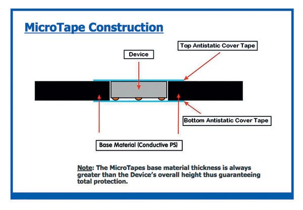
MicroTape design
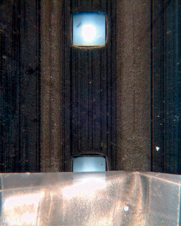
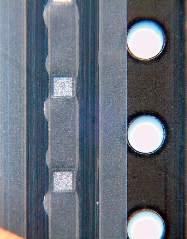
MicroTape is an engineered special carrier tape for WLP devices either in bare-die or flip-chip form factor. It exhibits high precision pockets with vertical walls not achievable using standard tape manufacturing processes, to provide absolute location for WLP devices. Base material thickness is selected to suit device thickness thus providing complete protection. Devices are located into the MicroTape pockets and retained using top and bottom cover tapes. Inspection of the device is possible as is the option to invert the device during the assembly process through the removal of either of the two cover tapes.
The evaluation and its results
The Siplace team conducted MicroTape pick-up and placement evaluation tests for small WLP devices. In order to evaluate the MicroTape solution a device measuring 0.7 x 0.7 mm (thickness 0.4 mm) was placed into MicroTape with a pocket size 0.8 x 0.8 mm (0.6 mm thick). The taping & reeling process was achieved with the use of Reel Service Ltd.’s high performance ISORT wafer to tape & reel systems. The ISORT automated equipment features electronic wafer map interpretation to preclude electrically failed devices from the taping & reeling process. Advanced vision capability provides for post-test screening of any mechanical defects down to 12 microns resolution including chipping, dicing issues, scratches, bump presence and contamination on both top side and bottom side of the WLP device. The result: There are only “known good die” (KGD) in the MicroTape pockets. A quantity of 3200 bare die devices were placed from one 7-inch reel using a Siplace X2 placement platform, equipped with a 20 nozzle Collect & Place head and standard 8-mm X-type component feeder. During the evaluation tests the 3200 bare die components were picked from the MicroTape and placed upon an examination board with 400 placement locations. A pick rate of 99.90 % was achieved at a placement rate of 21,000 cph.
The costs and what they say
From a technology-based point of view MicroTape, as described before, has many benefits. What must be considered in a production environment are the total costs for feeding a component into a pick & place system. At the first glance it may appear that MicroTape has a disadvantage when compared with direct wafer feeding solutions, since a certain amount has to be paid for wrapping each chip into a tape. However, when comparing the total costs of component feeding for different feeder (and packaging) alternatives, a clear dependency of the costs from the quantity placed per year and capital equipment cost factors provide influence to that first impression.
For comparison we defined the total costs of device feeding as the capital investment for the feeder mechanism, the costs for packaging (in case of flip chip or bare die the components being delivered as sawn wafers on foil in a film-frame have no packaging costs), the costs for lost components due to pick-up problems.
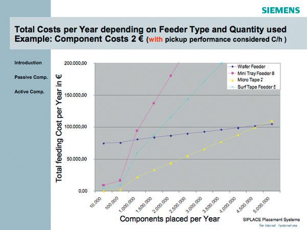
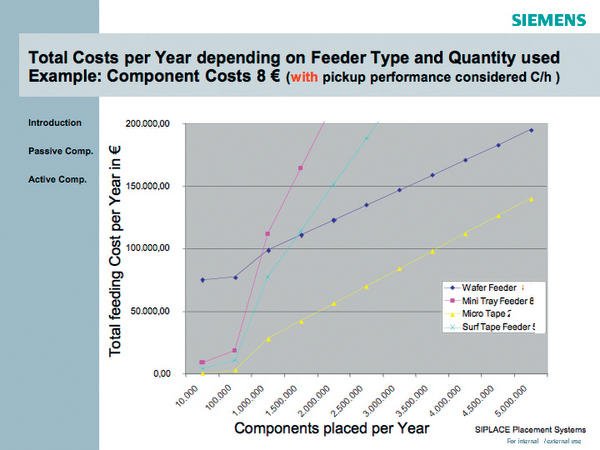
We skip the costs for maintaining the feeder unit, as it is difficult to predict those costs for the variety of different systems available in the market, but for wafer feeding systems which are typically complex, those costs are clearly not insignificant and an important adder that must be taken wholly into account for anyone considering such solutions. When looking at the initial costs for a feeder unit, the investment is calculated with depreciation over five years. To make the costs comparable, the performance of different feeder units has to be considered as well, since some feeder types may be able to deliver up 20.000 components per hour and others only a few thousand. Figure 3 and 4 show the impact of having different component prices on the break-even point when comparing different feeding methods. Under the assumption that wafer feeding, picking from a surf tape and picking out of a miniature tray have the same pick-up error-rate of 0.3 % and only MicroTape having a pick-up error-rate of 0.1 %, the break even between direct wafer feeding and MicroTape occurs at around 4.5 to 5 million components being placed.
Figure 4 displays that for very expensive components; it is very important to choose the most reliable feeding method having a very low pick-up error-rate.
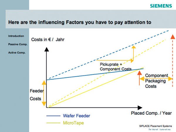
In Figure 5 the general impact of the three most important drivers for expenses is described. These are feeder costs, component packaging costs and pick-up-rate plus the component costs.
When comparing tape feeding with direct wafer feeding it has to be noted that beside cost considerations, the electronics manufacturer also has to consider that getting components packaged in tape adds one more station in the logistics chain. Depending upon whether the devices are received sawn on foil, or not, may extend general lead times. In practice the time difference between having wafers mounted on foil and sawn over mounted, sawn and taped & reeled components is negligible, thus favoring the tape option.
Conclusion and outlook
Siemens Electronics Assembly Systems concluded that MicroTape is well designed for high-speed-placement of components which need to be supplied within an accurate media and precise orientation. The use of standard feeder systems which usually already exist in a SMT assembly line makes for a solution which is both easy to use and straightforward for engineers to implement. This is generally a great improvement over alternative tape-based solutions which require to buy prohibitively high-cost, long lead-time ‘special’ feeder systems. High-speed SMT equipment using standard SMD placement platforms provides clear advantages for both ODMs and CEMs in reducing both assembly costs and capital equipment needs. Taped components provide for only ‘known good die’ and flip chips on assembly lines, negating the need to adjust quality assurance systems to accommodate both good and reject devices.
MicroTape, taped & reeled components are easier to handle than wafers or other adhesive-based tape material solutions providing for less component attrition due to handling problems. Where an assembly requires only a partial quantity of devices from a wafer, MicroTape provides a guaranteed method of future placement for remaining devices, ensuring that they may be used without the possibility of blue or UV film frame foil tearing, rendering them useless. For those users of multiple dies or flip chips on a single PCB or substrate assembly, standard placement machine feeder locations used with MicroTape enable multiple WLP device placement. And this is another advantage over die-bonder foil-based solutions where only one wafer may be accommodated and picked from at any one time.
EPP Europe 464
zusammenfassung
Der Einsatz von Wafer-Level Packaging erstreckt sich auf eine Vielzahl von Halbleiterbauelementen in einem Querschnitt von Industriezweigen vom Fahrzeugbereich über Mobiltelefone, Sensoren bis hin zur Medizintechnik. Diese Untersuchung zeigt, dass die Hochgeschwindigkeitsbestückung mit SMT-Standard-Plattformen klare Vorteile bietet, indem sie sowohl die Montagekosten als auch den Bedarf an Betriebsmitteln reduziert. MicroTape, gegurtete und gespulte Bauteile sind leichter zu handhaben als Wafer oder andere klebstoffbasierende Bandsysteme, indem sie für weniger Bauteilverlust infolge von Handlingproblemen sorgen.
L’utilisation de l’encapsulation sur tranches s’étend à de nombreux composants semi-conducteurs dans de nombreux secteurs industriels, allant de l’automobile à la technique médicale en passant par les téléphones portables et les capteurs. Cette étude démontre que le placement à haute vitesse à l’aide de plates-formes CMS standard offre de nets avantages, grâce à la réduction des coûts de montage et des besoins en moyens de production. Les composants MicroTape cerclés et bobinés sont plus faciles à manipuler que les tranches ou d’autres systèmes de rubans à base de colle, en réduisant la perte du composant à la suite de problèmes de manipulation.
L’adozione di wafer-level packaging si estende a un gran numero di elementi a semiconduttori in un settore dell’industria che va dagli autoveicoli ai telefoni cellulari, dai sensori alla tecnologia medicale. Questa ricerca evidenzia come il piazzamento ad alta velocità mediante piattaforme standard SMT offra evidenti vantaggi, riducendo nello stesso tempo i costi di montaggio e la necessità di mezzi di servizio. I componenti MicroTape, nastrati e in bobina, sono più facili da maneggiare rispetto a wafer o altri sistemi di nastratura basati su collante, riducendo nello stesso tempo la perdita del componente dovuta a problemi di manipolazione.
Bibliography and references
[1] Anon (2006): Flip Chip and Wafer Level Packaging, Trends and market Forecasts. Techsearch International, Austin Tx.
[2] Anon (2006): Study Shows Flip-Chip and Wafer-Level Package Use Expanding. Semiconductor International, 10/16/2006.
[3] Guilian G., Haba, B., Oganesian, V., Honer, K., Ovrutsky, D., Rosenstein, C., Axelrod, E., Hazanovich, F. and Aksenton (2007): Compliant Wafer Level Package for Enhanced Reliability. Tessera Inc., San Jose; in International Symposium on High Density Packaging and Microsystem Integration, 2007. HDP ’07.
[4] Heilmann, N (2008): Testing of pickup-rate and placement rate for bare die packaged in MicroTape. Siemens AG, Munich 2008.
[5] Patwardhan, V.; Chin, D.; Wong, S.; Rey, E.; Kelkar, N.; Nguyen, L. (2005): Flexural testing of board mounted wafer level packages for handheld devices. Electronic Components and Technology Conference, 2005. Proceedings. 55th Volume , Pp. 557 – 561 Vol. 1
Share:


