Lots of people are talking about 3D inspection or 3D AOI, and tossing the term around loosely, but in fact many different people have somewhat different perceptions of what ‘3D inspection’ actually is. We understand of course what ‘3D’ means – or do we? For example, it is commonplace now for many different equipment manufacturers to describe their inspection systems as having ‘3D inspection capability’. But that’s easy when the strict definition is not clearly understood. So what is behind the term ‘3D inspection’, and what are the different approaches to it currently being offered to the electronics manufacturing industry? What is true 3D capability and, to take matters one step even further, when does ‘3D inspection’ actually become ‘3D measurement’, and is that better?
Thorsten Niermeyer, Koh Young Technology, Dublin (Ireland)
A number of equipment vendors have successfully used 3D inspection capability for the purposes of measurement (metrology) for many years, but predominantly in the form of solder paste inspection (SPI) or, more correctly, solder paste measurement. It is necessary to differentiate between measurement and inspection, since 3D systems actually measure the solder paste volume deposited on individual substrate SMT pads. Deploying different measurement technologies such as laser triangulation or phase shift profilometry achieves reasonably good results in performing 3D volumetric measurement, but the task itself is relatively simple: it is just volumetric measurement of (essentially) rectangular printed deposits of uniformly grey solder paste.
The success of three-dimensional solder paste measurement during the last decade is proven through the process improvements that these systems have contributed to board-assembly manufacturing industry, particularly to the paste printing process. The adoption rate of 3D SPI systems in electronics production environments has grown from approximately 15% for all SMT lines a decade ago to now having reached market coverage of nearly 60%.
3D measurement
Whether the same measurement technologies used for solder paste can be applied to solder joints depends on the technology. Laser scanning technology has been tried unsuccessfully on soldered boards for many years by a few AOI system suppliers. The only proven technology in conducting real 3D measurements of solder joints is phase shift profilometry.
The task of measuring curved and highly reflective solder joints is complex; hence laser technology can’t be applied. The shiny surface and the multi-angled curvature of the solder joint mean that a laser can’t be used to map all areas. Similarly, when applying light as the part of the measurement technology regardless of LED or flash, white or multi-colored, specula reflection has to be overcome as an obstacle to obtaining information from certain regions. Multiple directions of light projections must be used in order to compensate for this specula reflection. Too few light directions will not allow for such compensation.
2D AOI
In the current debate, 2D AOI technology, which has been deployed for the last 25 years, can’t be overlooked. AOI systems with different technology approaches have been utilized in the industry for a quarter century. It was the only technology available to replace manual, human inspection of assembled PCBs. The fact that there are more than 25 AOI equipment supplier companies on the market illustrates the need and the importance of end-of-line or solder-joint inspection in electronics manufacturing. These systems and the technology have reached coverage beyond 90% of all SMT lines, and thus much more than that of SPI systems.
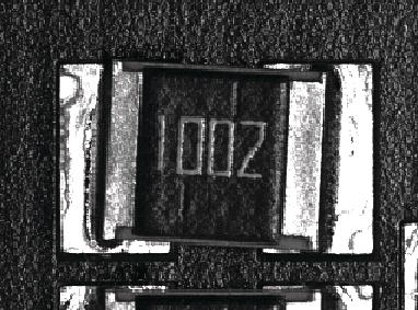
Since 2D systems deploy light from multiple angles onto the PCB, components and solder joints, all results for inspection are dependent on either contrast (e.g. location and polarity measurement) or location of reflection points (solder joint inspection).
Even when multiple camera or viewing angles are used, the results are still based on the availability of the applied light. Herein lies the problem; taller components will cast shadows onto other components and solder joints. The different lighting conditions resulting from shadowing require the AOI programmer to modify thresholds on a component-by-component basis. As the same type of components on the same board have different thresholds applied, this leads to different defect detection capability and varying amounts of false fails (or false calls).
3D measurement applications
First, let’s have a look at some relevant questions in the SMT line: Is 3D measurement applicable and really necessary for every aspect of the components and solder joints? Can certain attributes not be inspected in 2D, as they have been for many years? The advantages of three-dimensional measurement lie in the word measurement. If you can measure the volume of each and every visible solder joint of every component, why would you just satisfy yourself with counting the bright pixels that the solder curvature is reflecting from an angled light source?
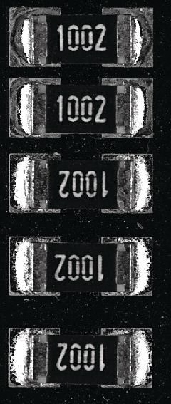
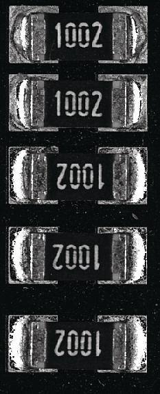
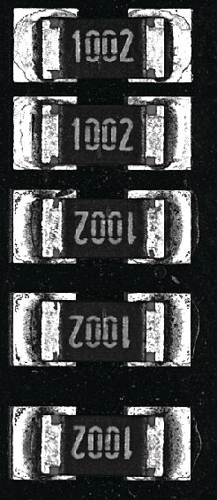
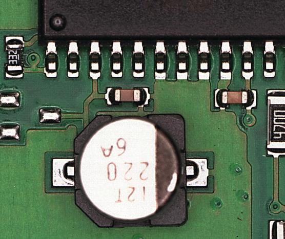
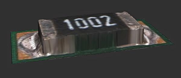
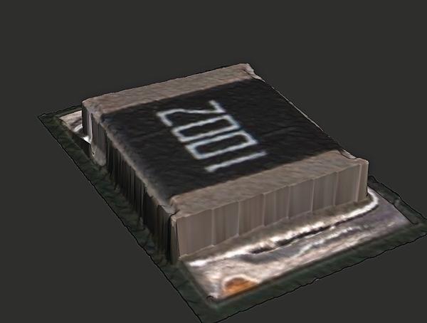
Why would one try to discriminate the edges of the component through different colors or grey scales, if one can measure the edge without the influence of component or PCB color in the third dimension? A typical scene of a chip resistor can be of varying color against the background of a PCB, which can also be of a different hue.
Current AOI vendors are offering a different level of 3D coverage for components and solder joints. All 3D systems still offer 2D lighting and 2D inspection. It is for the AOI programmer or the QA department to decide to what extend they’d like to deploy new technology for their quality assurance and process control. Contrary to commonly-held opinion, the polarity of components is typically a geometric feature rather than just a print. Those chamfers, dimples or corners can easily be measured in the third dimension, rather than relying on varying color and intensity of the print on the surface.
Replacement for 2D inspection?
Some AOI vendors hold the view that it is only necessary to measure certain aspects or characteristics of the component in 3D, such as component location. All other attributes would be inspected in the traditional 2D method. This approach is not coherent from a measurement perspective, since the solder joint is a three-dimensional structure as well, and a very complex.
Applying the lower level 2D technology to the most critical feature on the PCB, the solder joint, doesn’t make sense when 3D measurement is available. This split philosophy from AOI vendors can only be the result of technical machine limitations, rather than actual measurement requirements.
Improving quality
Applying 3D measurement to as many aspects of the components and solder joints on a PCB is the best approach to improving the quality assurance and process control of assembled PCBs, by utilizing true measurement technology with quantifiable measurement thresholds. For example, it is easy to understand that a lead is lifted for 170µm and hence is bad (out of range) if the applied threshold is 150µm. There is no more interpretation of this result necessary, no image processing knowledge required and certainly no room for false calls or false accepts. This allows translating quality requirements into AOI measurement thresholds. It makes these values transparent and understandable for everyone involved, e.g. the AOI programmer, the quality department and the operator at the AOI review station.
3D AOI has the ability to measure the Z-axis profilometry of whole assembled PCB surfaces based on the patented multifrequency Moiré technology. In traditional 2D AOI inspection, however, the inability to measure the height of objects makes detection of defects such as lifted leads and components difficult. True 3D AOI measurement eliminates false alarms, escapes and inspection errors, because the ability to measure the height and shape of components and shiny solder joints allows a true comparison with the IPC-A-610 standard for inspection. Thus, there is no question regarding the acceptability of the solder joint.
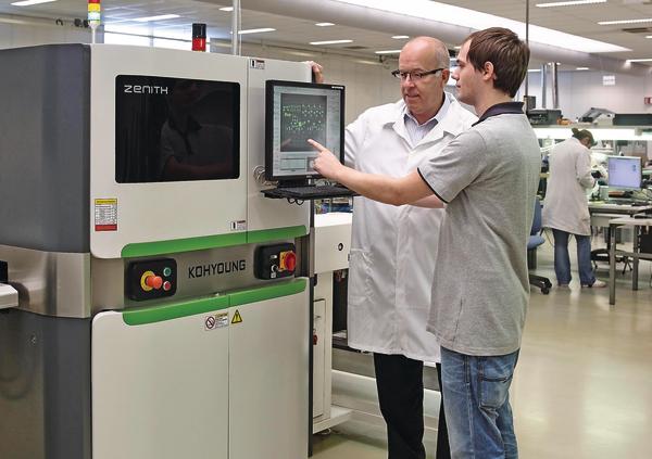
In the example of Koh Young’s flagship Zenith 3D AOI system, 2D and 3D information are utilized together for better visualization of the components and solder joints. The technology is thus easily integrated into an automated SMT line. 3D measurement technology cuts down on defective product getting into the field, minimizes scrap and waste as well as rework, slashes re-inspection costs and time wasted, and compensates for PCB warpage.
Conclusion
Increasing demands for higher yields with fewer false calls in the highly-competitive world of electronics manufacturing are met with the more powerful and advanced technology of 3D AOI measurement, where traditional 2D AOI inspection cannot provide the measurement capability required for quality assurance. 3D measurement technology is the perfect process optimization solution for ensuring better quality products, shorter cycle times, and across-the-board IPC-A-610 compliance. 3D measurement therefore is not just a buzzword, but the future technology for precise AOI. 3D has proven its capability and superiority over the existing 2D methods in volumetric solder paste measurement.
Productronica, Booth A2.377
Zusammenfassung
Als AOI in der Baugruppenfertigung vor über 25 Jahren begann Fuß zu fassen, handelte es sich um 2D-Systeme. Sie haben sich mehr oder weniger bewährt und sind in vielen Fertigungen zu finden. Doch wenn es um exakte Messungen für Prozesskontrolle und Qualitätssicherung geht, führt kein Weg an präzisen 3D-Systemen vorbei. Hier gibt es dann keine Ermessensspielräume und Interpretationen mehr, ob eine angezeigte Abweichung noch tolerierbar ist oder nicht.
Lorsque l’AOI a commencé à prendre pied il y a plus de 25 ans dans la production de composants, il s’agissait de systèmes 2D. Ils ont fait plus ou moins leurs preuves et se retrouvent dans diverses fabrications. Mais rien ne se fait sans des systèmes 3D précis s’il s’agit de mesures exactes pour le contrôle des processus. Elles ne laissent pas de marges d’appréciation et des interprétations pour savoir si l’écart indiqué est hors tolérance ou non.
Share:


