EKRA Automatisierungssysteme GmbH, a Member of the ASYS Group, is located in the High-Tech Mechanical Engineering Region Stuttgart. EKRA is a development and engineering company specialized on processes and systems for complex material deposition by printing. The company’s comprehensive know-how flows into many areas of daily life. Products built with our technology are ubiquitous. Whether in the kitchen, car, hospital, consumer electronics or power generation, EKRA’s printing solutions make a critical contribution in manufacturing.
One focus is on the ongoing miniaturisation of electronics. Ever smaller designs make it possible to penetrate new, previously unexplored areas. Miniaturisation requires new processes and equipment to be able to process such complex components.
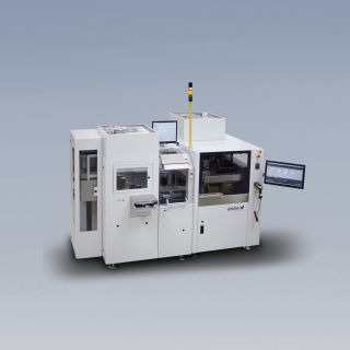
One of the hidden champions is the wafer printing cell. A highly efficient system for processing wafers. Depending on the process stage, the wafers can be coated over a wide area or tens of thousands of bumps can be printed.
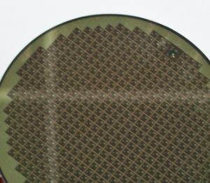
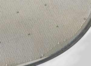
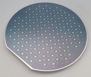
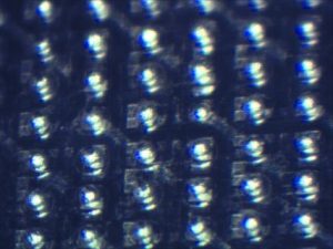
The flexible machining cell is designed for front or back side printing (bumping or wafer backside coating) on round wafers. The system consists of two main modules, a loading unit and a printing system. The loading unit consists of three components: a magazine unloading system, a robot unit and a pre-alignment station. The magazine unloading system is equipped with two magazine positions from where the wafers are fed to the machine. The 3-axis robot unit with vacuum suction pad ensures a stress-free wafer transport. Using a flexible pick-up, different end effectors can be used even for very thin or curved wafers. After the wafer is removed from the magazine, it is repositioned in the pre-alignment station by flat or notch detection for subsequent printing. Now, the wafer is placed on dedicated elevation pins of the vacuum print nest and then lowered and fixed. The print nest is transported into the printer. Then the register marks are detected by the free-moving camera and the screen or stencil is aligned to the wafer. The printing process is then carried out. The printed wafer is now transported back into a magazine or can be removed individually with a drawer system.
Subsequent process steps, such as heat treatment, can be integrated in or on the cell at the customer’s request.