In several Industry sectors we hear more often about a paradigm shift from globalization to regionalization. Some major, global Semiconductor Companies have recently announced to make huge investments in a next- generation European chip ecosystem.
Until now, Semiconductor business in Europe has been a niche in a fast-growing global Industry sector. Hence most EU manufacturing environments are based on very flexible, low quantity supply chains based on legacy processes for small batches.
Chip designers are thinking more often in platform structures to reduce development cycles and improve time to market. Combined with growing quantities this is going to offer plenty of opportunities to improve productivity and efficiency for European Semiconductor Manufacturing.
To be able to migrate from SMD to Semiconductor packaging a knowledge transfer in several areas of the supply chain is going to take place. Soon many SMD manufacturer will also produce components and supposed to be able to manufacture mid-size or even high quantity batches.
With this newsletter we like to support SMD and Semiconductor manufacturing with information about very efficient, high performance print processes for Semiconductor Packaging.
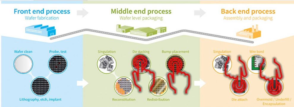
In the coming months we will share experience specifically about the following topics:
• Bumping
• Balling
• Flux printing
• Chip assembly
• Chip stack assembly
• Pre-bowed Chip assembly
• Copper Pillar chip assembly
• Chip moulding and filling
• Conventional LED assembly
• Min-LED assembly
All those advanced precision printing processes can be supported with high precision printing Tools and well-defined Process Parameters.
We are looking forward to a fruitful dialogue about continues process improvements and like to invite you to join us to this series of advanced manufacturing methods for Semiconductor Backend processes.