To be able to migrate from precision placement of SMD to Semiconductor packaging a knowledge transfer in several areas of the supply chain is going to take place. We believe that soon many SMD manufacturer will also produce components and supposed to be able to manufacture mid-size or even high quantity batches.
With this newsletter we like to support SMD and Semiconductor manufacturing with information about very efficient, high performance print processes for Semiconductor Packaging. In the coming months we will share experience specifically about the following topics:
Semiconductor Backend Processes
• Bumping
• Balling
• Flux printing
• Chip assembly
• Chip stack assembly
• Pre-bowed Chip assembly
• Copper Pillar chip assembly
• Chip moulding and filling
• Conventional LED assembly
• Min-LED assembly
Wafer Bumping Process
This bump technology has some advantages over wire bonding. It can make much shorter electrical connection then wire and achieve better electrical performance. It also can make array with much more I/O accounts means it can process much more data than wire. The wafer bumping process is made for whole wafers to be metalized at one-time, so-called batch process, means this process is much faster than wire bonding. It can end up with lower cost for wafer level CSP (Chip Scale Package) with lower process cost.
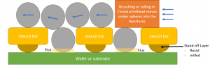
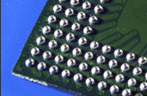
There are two major bumping types. One is solder bump and the other one is cupper pillar bump. Usually solder bump (Wafer Bumping) is used for coarse pitch more than 150µm and cupper pillar fine pitch for less than 150µm. This numbers are based on experience and does not mean to be an absolute rule. Wafer Bumping is a common process to generate „Flip Chip“ Bumps on the Wafer Backsite (Components) or on a substrate ( SIP,Chiplets,WLFO , Modules).
This bumps are needed to make the interconnection between the single component or the package to the PCB or even between the Die stacks in the package.
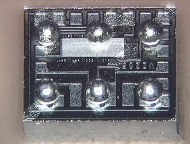
The wet solder paste gets placed on the Wafer or substrate followed by a reflow process. During the reflow process, the paste will reach the liquidus phase and the surface tension of the solder metal will form a circle segment. (called „BUMP“ )
In order to avoid issues due to unreliable co-planarity in the assembly process, the consistent height of each bump is one of the key performance indicators of this process.
The height of each bump gets determined by the size of the UBM (Under Bump Metallization) and the volume of the paste deposit. The Paste height and volume is very much depending on the paste and the precision printing tools.
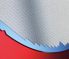
At Christian Koenen we have developed a specific process on special dedicated Laser Machines to ensure a very small tolerance in terms of Aperture size and shape. Together with dedicated and selected Materials for all our bumping stencils we can ensure a very small tolerance band in terms of bump height. This is very important for either 100 bumps on a substrate or even >600.000 bumps on a Wafer.
